AMD Plans Massive Memory Instinct MI325X for Q4'24, Lays Out Accelerator Roadmap to 2026
by Ryan Smith on June 2, 2024 11:02 PM EST- Posted in
- GPUs
- AMD
- AMD Instinct
- AI
- CDNA
- Computex 2024
- CDNA 4
- CDNA Next
- MI350
- MI400
In a packed presentation kicking off this year’s Computex trade show, AMD CEO Dr. Lisa Su spent plenty of time focusing on the subject of AI. And while the bulk of that focus was on AMD’s impending client products, the company is also currently enjoying the rapid growth of their Instinct lineup of accelerators, with the MI300 continuing to break sales projections and growth records quarter after quarter. It’s no surprise then that AMD is looking to move quickly then in the AI accelerator space, both to capitalize on the market opportunities amidst the current AI mania, as well as to stay competitive with the many chipmakers large and small who are also trying to stake a claim in the space.
To that end, as part of this evening’s announcements, AMD laid out their roadmap for their Instinct product lineup for both the short and long term, with new products and new architectures in development to carry AMD through 2026 and beyond.
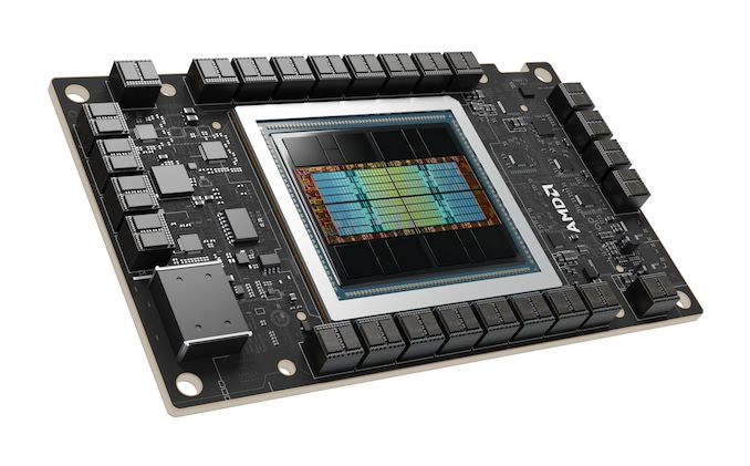
On the product side of matters, AMD is announcing a new Instinct accelerator, the HBM3E-equipped MI325X. Based on the same computational silicon as the company’s MI300X accelerator, the MI325X swaps out HBM3 memory for faster and denser HBM3E, allowing AMD to produce accelerators with up to 288GB of memory, and local memory bandwidths hitting 6TB/second.
Meanwhile, AMD also showcased their first new CDNA architecture/Instinct product roadmap in two years, laying out their plans through 2026. Over the next two years AMD will be moving very quickly indeed, launching two new CDNA architectures and associated Instinct products in 2025 and 2026, respectively. The CDNA 4-powered MI350 series will be released in 2025, and that will be followed up by the even more ambitious MI400 series in 2026, which will be based on the CDNA "Next" architecture.
AMD Instinct MI325X: Maximum Memory Monster
Starting things off, let’s take a look at AMD’s updated MI325X accelerator. As with several other accelerator vendors (e.g. NVIDIA’s H200), AMD is releasing a mid-generation refresh of their MI300X accelerator to take advantage of the availability of newer HBM3E memory. Itself a mid-generation update to the HBM standard, HBM3 offers both higher clockspeeds and greater memory densities.
Using 12-Hi stacks, all three of the major memory vendors are (or will be) shipping 36GB stacks of memory, which is 50% greater capacity than their current top-of-the-line 24GB HBM3 stacks. Which for the 8 stack MI300 series, will bring it from a maximum memory capacity of 192GB to a whopping 288GB on a single accelerator.
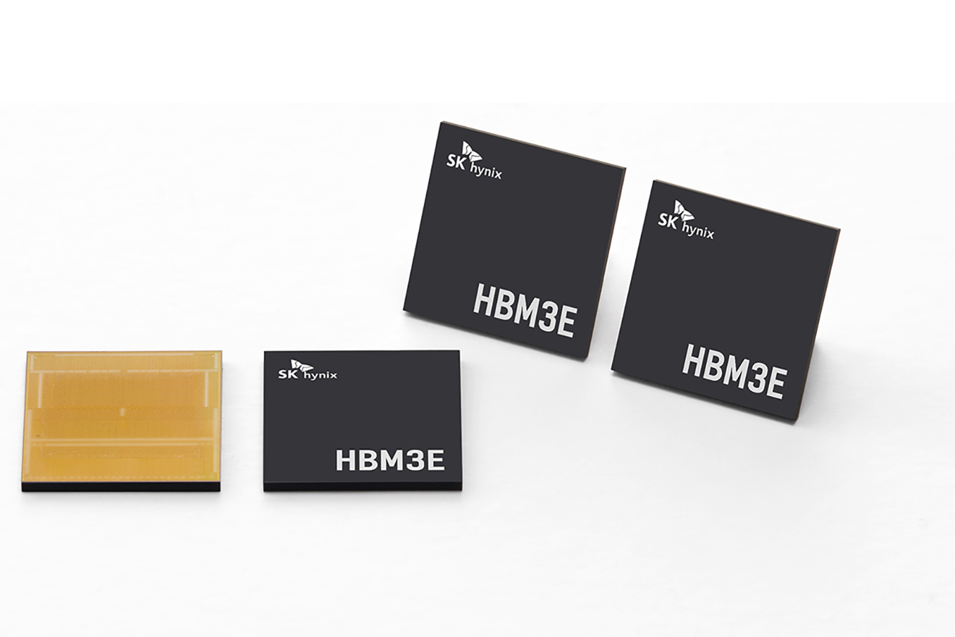
HBM3E brings faster memory clockspeeds as well. Micron and SK hynix expecting to eventually sell stacks that clock as high as 9.2Gbps/pin, and Samsung wants to go to 9.8Gbps/pin, over 50% faster than the 6.4Gbps data rate of regular HBM3 memory. With that said, it remains to be seen if and when we’ll see products using memory running at those speeds – we’ve yet to see an accelerator run HBM3 at 6.4Gbps – but regardless, HBM3E will afford chip vendors more badly-needed memory bandwidth.
| AMD Instinct Accelerators | ||||||
| MI325X | MI300X | MI250X | MI100 | |||
| Compute Units | 304 | 304 | 2 x 110 | 120 | ||
| Matrix Cores | 1216 | 1216 | 2 x 440 | 480 | ||
| Stream Processors | 19456 | 19456 | 2 x 7040 | 7680 | ||
| Boost Clock | 2100MHz | 2100MHz | 1700MHz | 1502MHz | ||
| FP64 Vector | 81.7 TFLOPS | 81.7 TFLOPS | 47.9 TFLOPS | 11.5 TFLOPS | ||
| FP32 Vector | 163.4 TFLOPS | 163.4 TFLOPS | 47.9 TFLOPS | 23.1 TFLOPS | ||
| FP64 Matrix | 163.4 TFLOPS | 163.4 TFLOPS | 95.7 TFLOPS | 11.5 TFLOPS | ||
| FP32 Matrix | 163.4 TFLOPS | 163.4 TFLOPS | 95.7 TFLOPS | 46.1 TFLOPS | ||
| FP16 Matrix | 1307.4 TFLOPS | 1307.4 TFLOPS | 383 TFLOPS | 184.6 TFLOPS | ||
| INT8 Matrix | 2614.9 TOPS | 2614.9 TOPS | 383 TOPS | 184.6 TOPS | ||
| Memory Clock | ~5.9 Gbps HBM3E | 5.2 Gbps HBM3 | 3.2 Gbps HBM2E | 2.4 Gbps HBM2 | ||
| Memory Bus Width | 8192-bit | 8192-bit | 8192-bit | 4096-bit | ||
| Memory Bandwidth | 6TB/sec | 5.3TB/sec | 3.2TB/sec | 1.23TB/sec | ||
| VRAM | 288GB (8x36GB) |
192GB (8x24GB) |
128GB (2x4x16GB) |
32GB (4x8GB) |
||
| ECC | Yes (Full) | Yes (Full) | Yes (Full) | Yes (Full) | ||
| Infinity Fabric Links | 7 (896GB/sec) |
7 (896GB/sec) |
8 | 3 | ||
| TDP | 750W? | 750W | 560W | 300W | ||
| GPU | 8x CDNA 3 XCD | 8x CDNA 3 XCD | 2x CDNA 2 GCD | CDNA 1 | ||
| Transistor Count | 153B | 153B | 2 x 29.1B | 25.6B | ||
| Manufacturing Process | XCD: TSMC N5 IOD: TSMC N6 |
XCD: TSMC N5 IOD: TSMC N6 |
TSMC N6 | TSMC 7nm | ||
| Architecture | CDNA 3 | CDNA 3 | CDNA 2 | CDNA (1) | ||
| Form Factor | OAM | OAM | OAM | PCIe | ||
| Launch Date | Q4'2024 | 12/2023 | 11/2021 | 11/2020 | ||
Matrix throughput figures for dense (non-sparse) operations, unless otherwise noted
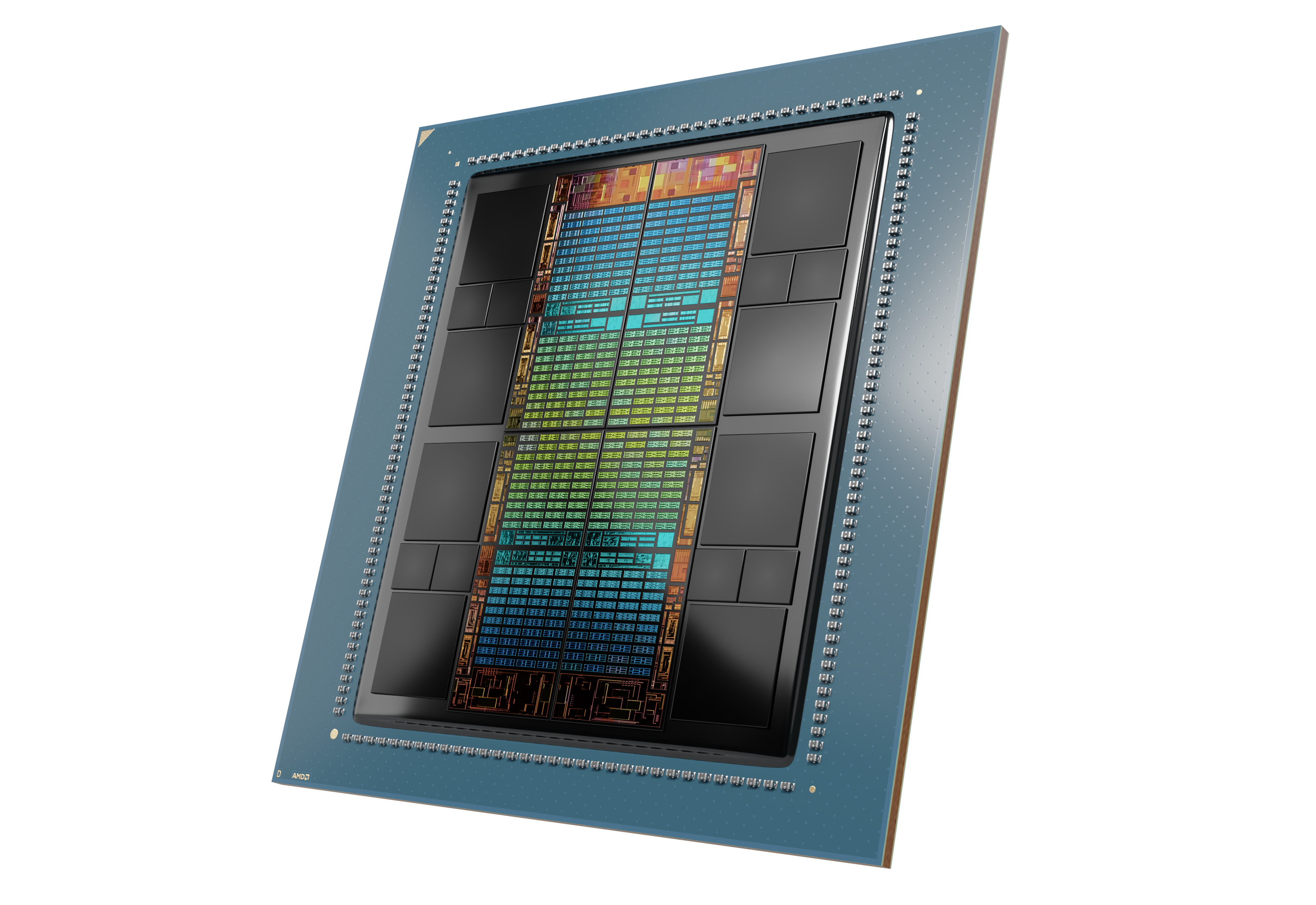
Diving into the specifications for the MI325X, we find that, other than the memory swap, it remains unchanged from the original CDNA 3 architecture MI300X. AMD is still using their same 8 XCD + 4 IOD configuration here, which affords the chip 1216 matrix cores and a maximum throughput at INT8 of 2614 TOPS. Given AMD’s throughput claims, it looks like clockspeeds have not changed from the MI300X’s 2.1GHz, so this is a straightforward memory upgrade SKU.
Notably here, even with the switch to HBM3E, AMD isn’t increasing their memory clockspeed all that much. With a quoted memory bandwidth of 6TB/second, this puts the HBM3E data rate at about 5.9Gbps/pin. Which to be sure, is still a 13% memory bandwidth increase (and with no additional compute resources vying for that bandwidth), but AMD isn’t taking full advantage of what HBM3E is slated to offer. Though as this is a refit to a chip that has an HBM3 memory controller at its heart, this isn’t too surprising.
The bigger reason to use HBM3E in this case is its memory capacity. At 288GB of local RAM, this upgrade pushes the MI250X even farther ahead in terms of memory capacity per accelerator. And, in what AMD considers a crucial threshold, it will give an 8-way configuration 2.3TB of RAM – enough to run a trillion parameter LLM on a single server node. It goes without saying that LLMs have been living up to their names, so a big part of the race for AI accelerators has been how much of a model a single node can hold, and how much bigger a large cluster can go.
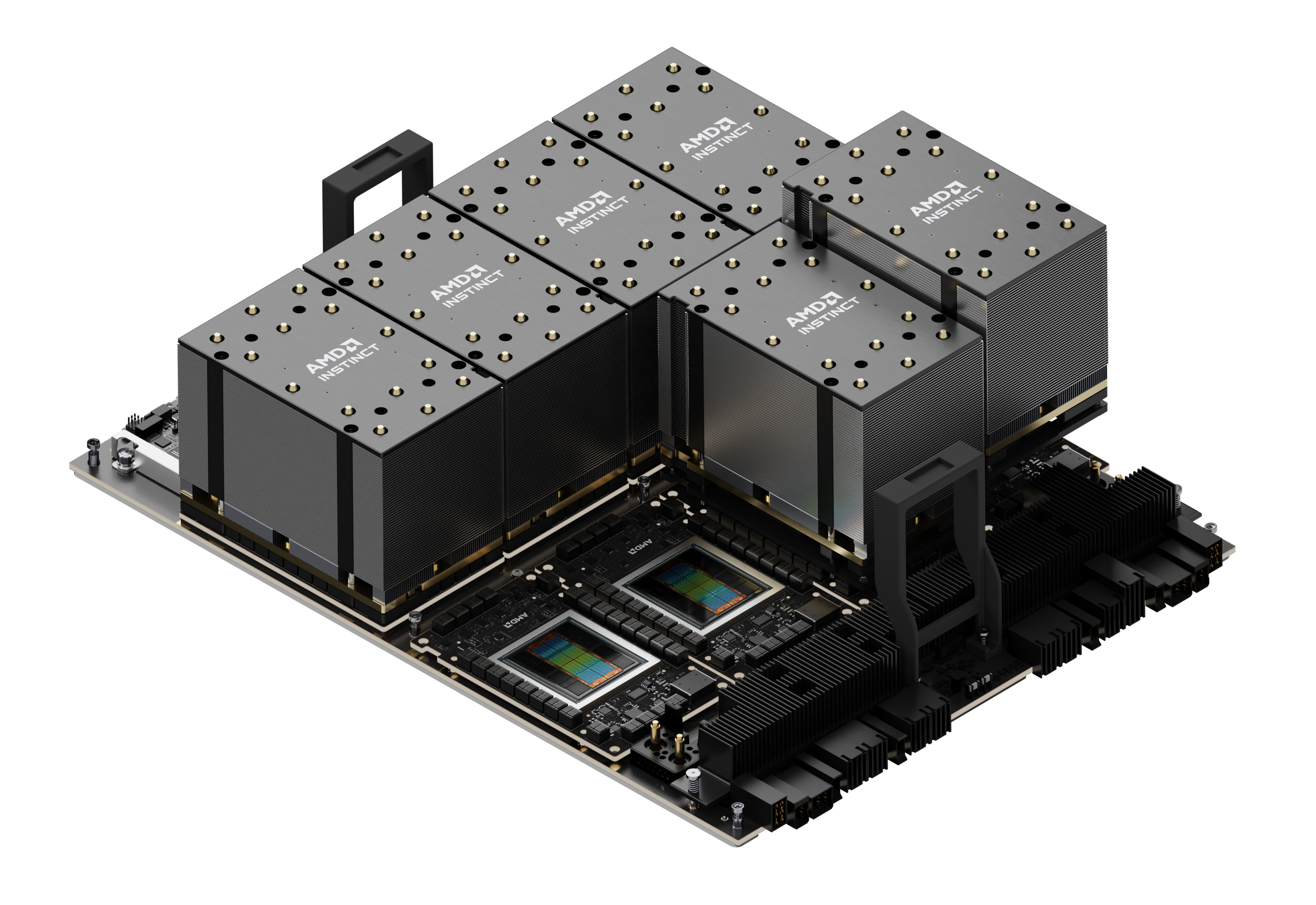
MI325X will otherwise fit in to AMD’s existing MI300X infrastructure, including their 8-way OAM universal baseboard. The company has not quoted a TDP for the new parts (faster memory tends to come with higher power consumption), but as the XCD clockspeeds haven’t changed, we aren’t expecting any big shifts from the MI300X’s 750W TDP.
The Instinct MI325X is slated to launch in Q4 of this year. AMD isn’t offering any sales projections right now (and that’s more a financial analyst matter to begin with), but it should be noted that AMD is going to be competing with the rest of the industry for valuable and limited HBM3 capacity. Micron has already sold out its 2024 supply (and most of 2025), and the other HBM vendors aren’t far behind. So don’t expect the MI300X to go anywhere so long as HBM3E remains in tight supply.
A Q4 launch also puts AMD on a collision course with NVIDIA’s next-generation B200 Blackwell accelerator, which as of its announcement at GTC 2024 in April, was scheduled to launch by the end of 2024. The ramp-up time for an entirely new accelerator means that AMD is likely going to beat NVIDIA to market – and regardless of timing, they’ll have the advantage in local accelerator memory capacity – but it does mean that MI325X will eventually have to fend off some next-generation competition as well.
On a side note, we did get a chance to ask AMD about any other forthcoming Instinct MI300 series products. In particular, a PCIe version of the accelerator remains notably absent. While AMD is aware of the interest, they aren’t bringing a PCIe card to market right now – and reading between the lines, it sounds like they’re already selling everything they can make as OAM modules. Which would mean there’s little incentive to offer slower (and potentially lower margin) PCIe cards.
AMD CDNA Architecture Roadmap: 3nm CDNA 4 in 2025, CDNA Next in 2026
Besides AMD’s immediate product plans for the upgraded Instinct MI325X, the company is also using this year’s Computex to offer a fresh look at their long-term CDNA architecture/Instinct product roadmap, which was last updated in 2022 and only went through the end of last year (the CDNA 3/MI300 launch). AMD has previously already confirmed that they’ve been working on a CDNA 4 architecture, but this is the first time it’s been roadmapped and described in any detail. Meanwhile the roadmap also adds a further CDNA architecture after that, CDNA "Next" (the presumptive CDNA 5), which will be released in 2026.
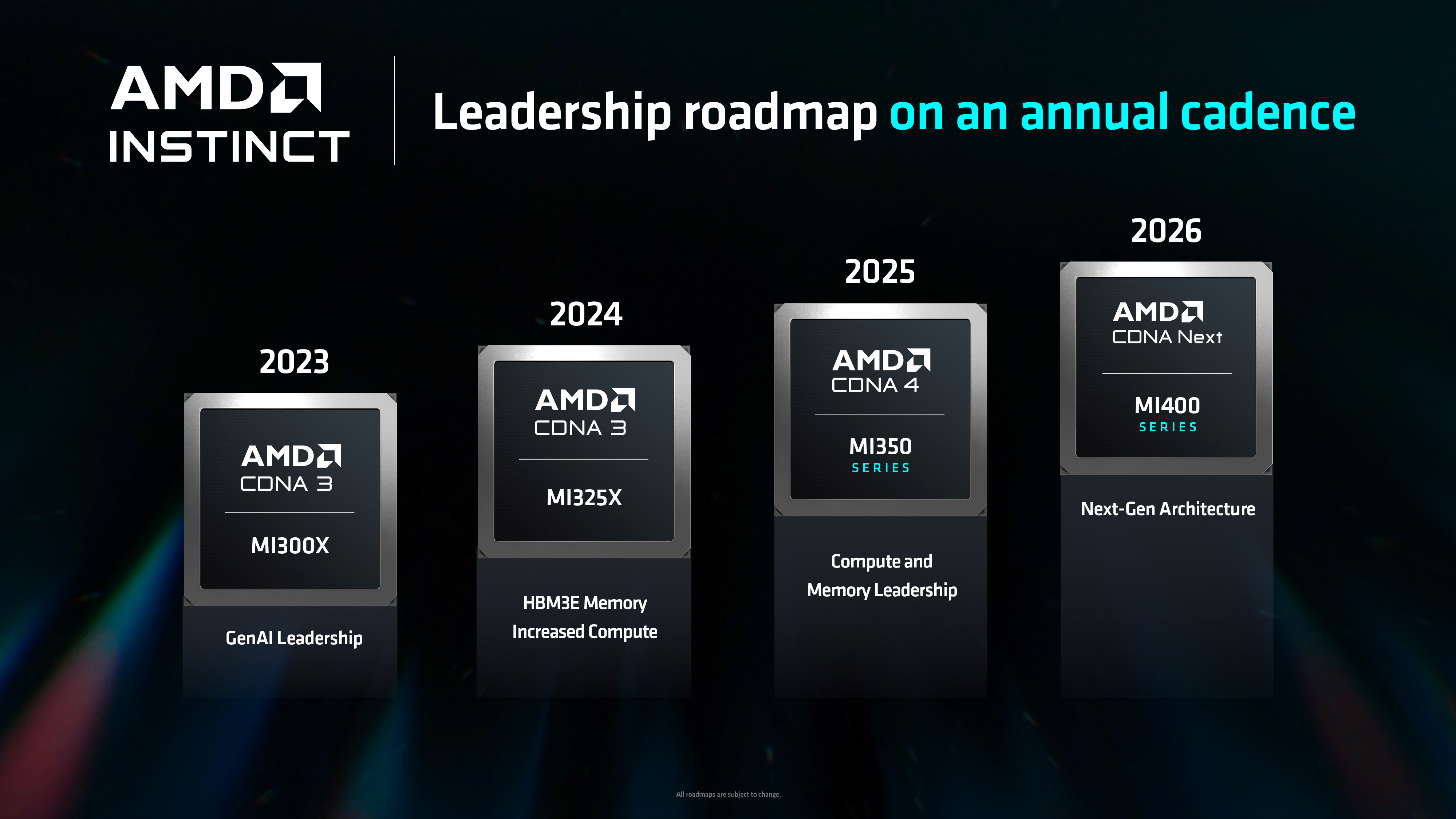
The CDNA 4 architecture will be the heart of AMD's MI350 series accelerators, which are slated to arrive in 2025. With the new architecture, AMD is aiming to hold on to their “memory leadership,” (which we infer to mean memory capacity leadership), as well as increased compute performance.
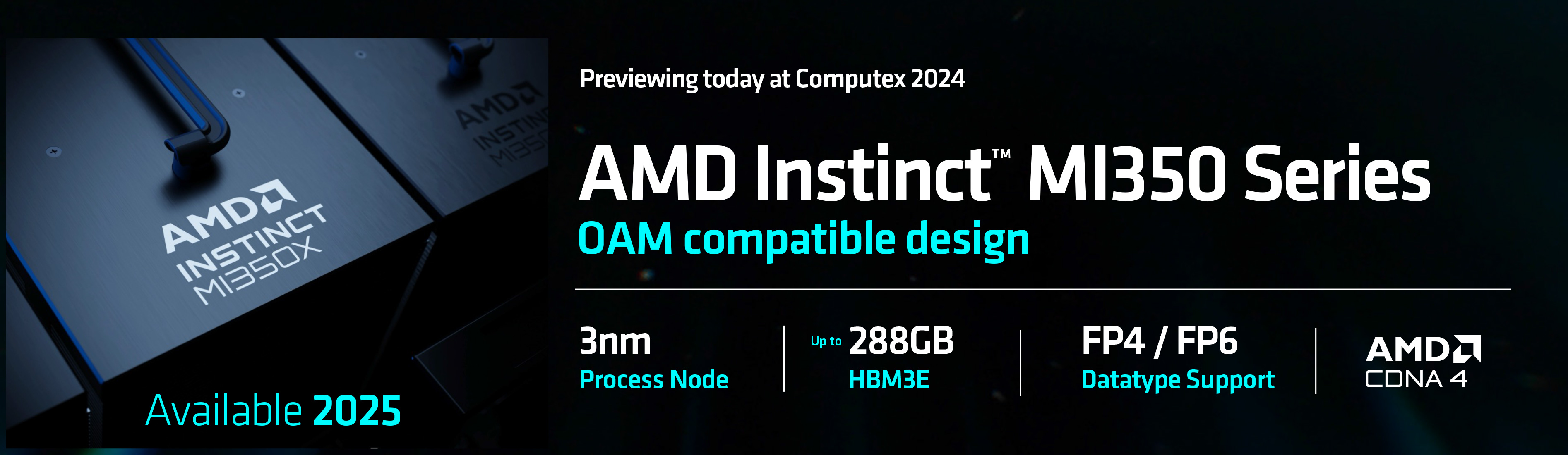
CDNA 4 architecture compute chiplets will be built on a 3nm process. AMD isn’t saying whose, but given their incredibly close working relationship with TSMC and the need to use the best thing they can get their hands on, it would be incredibly surprising if this were anything but one of the flavors of TSMC’s N3 process. Compared to the N5 node used for the CDNA 3 XCDs, this would be a full node improvement for AMD, so CDNA 4/MI350 will come with expectations of significant improvements in performance and energy efficiency. Meanwhile AMD isn’t disclosing anything about the underlying IO dies (IOD), but it’s reasonable to assume that will remain on a trailing node, perhaps getting bumped up from N6 to N5/N4.
AMD is also planning on making expanded use of chiplets overall with the CDNA 4 architecture. Though it remains unclear as to just what that will entail.
Architecturally, AMD is revealing today that CDNA 4 will bring with it native support for even lower precision data formats – FP4 and FP6 – matching similar announcements from other vendors. As was the case with the introduction of INT8/FP8 support, bringing native support for even lower precision formats allows for a further boost to compute throughput in terms of operations per second, as well as reduced memory pressure through the smaller data sizes of the formats. LLM inference remains constrained by the memory capacity of AI accelerators, so there’s a good deal of pressure on the ecosystem to keep memory usage down with inference.
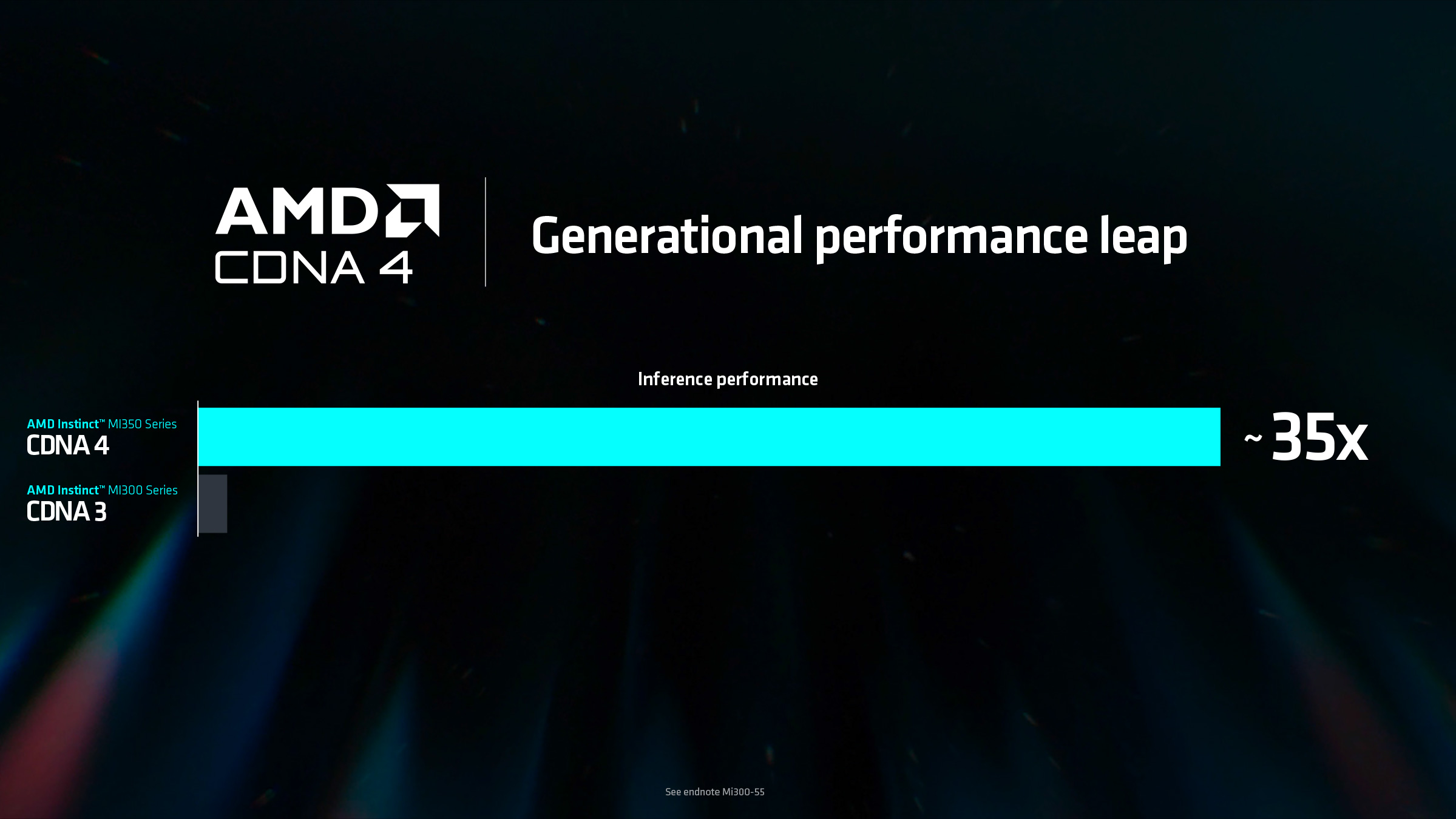
In terms of performance, AMD is touting a 35x improvement in AI inference for MI350 over the MI300X. Checking AMD's footnotes, this claim is based on comparing a theoretical 8-way MI350 node versus existing 8-way MI300X nodes, using a 1.8 trillion parameter GPT MoE model. Presumably, AMD is taking full advantage of FP4/FP6 here, as well as the larger memory pool. In which case this is likely more of a proxy test for memory/parameter capacity, rather than an estimate based on pure FLOPS throughput.
Meanwhile, those CDNA 4 compute chiplets will be paired with HBM3E memory, just as MI325X will be later this year. AMD isn’t announcing memory clockspeeds (though those will certainly be higher), but they are already revealing that MI350 accelerators will come with up to 288GB of memory, all but guaranteeing that the top-end CDNA 4 accelerators will once again use 8 stacks of memory.
Reading between the lines, it sounds like the CDNA 4 architecture will be a relatively straightforward upgrade of CDNA 3 that adds FP4/FP6 support without greatly altering the underlying compute architecture. AMD's decision to brand it as another MI300-series product, rather than jumping to MI400, seems to be a very intentional decision for a company that in other product segments (e.g. consumer) will iterate product numbers at the drop of a hat.
Finally, following CDNA 4 in 2025 will be AMD’s CDNA "Next” architecture in 2026, which will be used to power the MI400 series of accelerators. At two years out, AMD is offering fewer details here. But the company is emphasizing that it will offer a “significant” architectural upgrade over CDNA 4. With that description, and the full product bump to the MI400 series, it sounds like we should be expecting some major changes to the core computing architecture. That would be an especially notable development, as CDNA 3 (and presumably CDNA 4) can trace its ISA roots directly back to the 2017 GCN 5 (Vega) architecture.
Overall, AMD is publicly committing to an annual CDNA roadmap cadence starting in 2024, bumping things up from what has been a 2-year cadence for CDNA up to that point. This shift to a more rapid product schedule reflects AMD’s rising fortunes (and rapid growth) in the accelerator industry. Though it will be interesting to see just how well they can sustain it, given the high costs of developing cutting-edge chips. Still, with rival NVIDIA making a similar announcement not 24 hours earlier, the race in the accelerator industry is clearly itself accelerating.


3 Comments
View All Comments
ballsystemlord - Monday, June 3, 2024 - link
That 35x performance boost looks to be every bit as misleading as the gamer focused GPU metrics given by Nvidia over the years.ET - Monday, June 3, 2024 - link
Although the text and table show the 325X to have the same compute as 300X, the slide says "HBM3E Memory, Increased Compute".Dante Verizon - Monday, June 3, 2024 - link
Isn't the main bottleneck in AI bandwidth?