NVIDIA's Fermi: Architected for Tesla, 3 Billion Transistors in 2010
by Anand Lal Shimpi on September 30, 2009 12:00 AM EST- Posted in
- GPUs
Architecting Fermi: More Than 2x GT200
NVIDIA keeps referring to Fermi as a brand new architecture, while calling GT200 (and RV870) bigger versions of their predecessors with a few added features. Marginalizing the efforts required to build any multi-billion transistor chip is just silly, to an extent all of these GPUs have been significantly redesigned.
At a high level, Fermi doesn't look much different than a bigger GT200. NVIDIA is committed to its scalar architecture for the foreseeable future. In fact, its one op per clock per core philosophy comes from a basic desire to execute single threaded programs as quickly as possible. Remember, these are compute and graphics chips. NVIDIA sees no benefit in building a 16-wide or 5-wide core as the basis of its architectures, although we may see a bit more flexibility at the core level in the future.
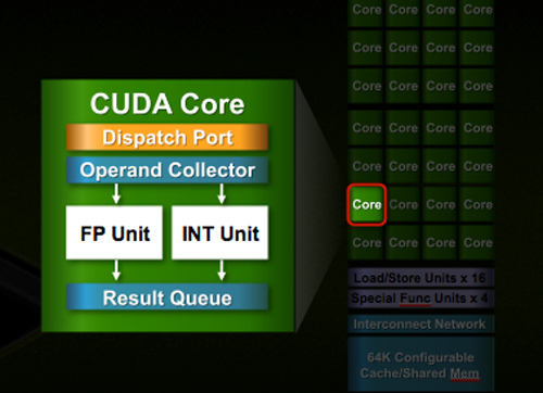
Despite the similarities, large parts of the architecture have evolved. The redesign happened at low as the core level. NVIDIA used to call these SPs (Streaming Processors), now they call them CUDA Cores, I’m going to call them cores.

All of the processing done at the core level is now to IEEE spec. That’s IEEE-754 2008 for floating point math (same as RV870/5870) and full 32-bit for integers. In the past 32-bit integer multiplies had to be emulated, the hardware could only do 24-bit integer muls. That silliness is now gone. Fused Multiply Add is also included. The goal was to avoid doing any cheesy tricks to implement math. Everything should be industry standards compliant and give you the results that you’d expect.
Double precision floating point (FP64) performance is improved tremendously. Peak 64-bit FP execution rate is now 1/2 of 32-bit FP, it used to be 1/8 (AMD's is 1/5). Wow.
NVIDIA isn’t disclosing clock speeds yet, so we don’t know exactly what that rate is yet.
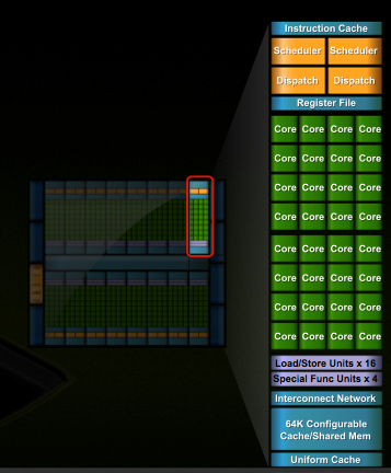
In G80 and GT200 NVIDIA grouped eight cores into what it called an SM. With Fermi, you get 32 cores per SM.

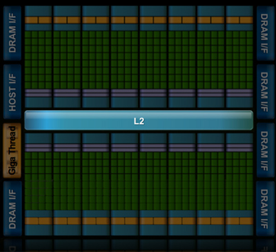
The high end single-GPU Fermi configuration will have 16 SMs. That’s fewer SMs than GT200, but more cores. 512 to be exact. Fermi has more than twice the core count of the GeForce GTX 285.
| Fermi | GT200 | G80 | |
| Cores | 512 | 240 | 128 |
| Memory Interface | 384-bit GDDR5 | 512-bit GDDR3 | 384-bit GDDR3 |
In addition to the cores, each SM has a Special Function Unit (SFU) used for transcendental math and interpolation. In GT200 this SFU had two pipelines, in Fermi it has four. While NVIDIA increased general math horsepower by 4x per SM, SFU resources only doubled.
The infamous missing MUL has been pulled out of the SFU, we shouldn’t have to quote peak single and dual-issue arithmetic rates any longer for NVIDIA GPUs.
NVIDIA organizes these SMs into TPCs, but the exact hierarchy isn’t being disclosed today. With the launch's Tesla focus we also don't know specific on ROPs, texture filtering or anything else related to 3D graphics. Boo.
A Real Cache Hierarchy
Each SM in GT200 had 16KB of shared memory that could be used by all of the cores. This wasn’t a cache, but rather software managed memory. The application would have to knowingly move data in and out of it. The benefit here is predictability, you always know if something is in shared memory because you put it there. The downside is it doesn’t work so well if the application isn’t very predictable.
Branch heavy applications and many of the general purpose compute applications that NVIDIA is going after need a real cache. So with Fermi at 40nm, NVIDIA gave them a real cache.
Attached to each SM is 64KB of configurable memory. It can be partitioned as 16KB/48KB or 48KB/16KB; one partition is shared memory, the other partition is an L1 cache. The 16KB minimum partition means that applications written for GT200 that require 16KB of shared memory will still work just fine on Fermi. If your app prefers shared memory, it gets 3x the space in Fermi. If your application could really benefit from a cache, Fermi now delivers that as well. GT200 did have an L1 texture cache (one per TPC), but the cache was mostly useless when the GPU ran in compute mode.

The entire chip shares a 768KB L2 cache. The result is a reduced penalty for doing an atomic memory op, Fermi is 5 - 20x faster here than GT200.


415 Comments
View All Comments
Fortesting - Wednesday, October 7, 2009 - link
See this article:http://www.semiaccurate.com/2009/10/06/nvidia-kill...">http://www.semiaccurate.com/2009/10/06/...x260-aba...
Zool - Tuesday, October 6, 2009 - link
Maybe tesla cards in supercomputers which are closed platforms the cuda is better but for anything other commercial OpenCL will be better.This is a CUDA vs OpenCL test from Sisoftware http://www.sisoftware.net/index.html?dir=qa&lo...">http://www.sisoftware.net/index.html?di...ocation=...
The conclusion from that article : We see little reason to use proprietary frameworks like CUDA or STREAM once public drivers supporting OpenCL are released - unless there are features your code depends on that are not included yet; even then, they will most likely be available as extensions (similar to OpenGL) pretty soon.
It wouldnt be bad to see those kind of tests on anadtech. Something like GPUs vs CPUs tests with same code.
Zool - Monday, October 5, 2009 - link
I dont know how others, but the 8 time increase in DP which is one of the pr stunts doesnt seem too much if u dont compare it to the weak gt200 DP numbers. The 5870 has something over 500 GFlops DP and the gt200 had around 80 GFlops DP (but the quadro and tesla cards had higher shader clocks i think). They will be happy if they reach 1.5 times the radeon 5800 DP performance. In this pdf from nvidia site http://www.nvidia.com/content/PDF/fermi_white_pape...">http://www.nvidia.com/content/PDF/fermi...T.Halfhi... they write that the ECC will hawe a performance penalty from 5% to 20% (on tesla cards u will hawe the option to turn it off/on on GT cards it will be turned off).Zool - Monday, October 5, 2009 - link
I also want to add that if the DP has increased 8 times from gt200 than let we say around 650 Gflops, than if the DP is half of the SP (as they state) performance in Fermi than i get 1300 Gflops ???? (with same clock speeds). For GT200 they stated 933 Gflops. Something is wrong here maybe ?Zool - Monday, October 5, 2009 - link
Actualy they state 30 FMA ops per clock for 240 cuda cores in gt200 and 256 FMA ops per clock for 512 cuda cores in Fermi. Which means clock for clock and core for core they increased 4 times the DP performance.SymphonyX7 - Saturday, October 3, 2009 - link
Hi. I'm a long time Anandtech reader (roughly 4 years already). I registered yesterday just because I wanted to give SiliconDoc a piece of my mind but thankfully ended being up being rational and not replying anymore.Now that he's gone. I just want to know what you guys think of Fermi being another big chip. Is it safe to assume that Nvidia is losing more money than ATI on high-end models being sold simply because the GTX cards are much bigger than their ATI counterparts? Moreso now that the HD 58xx cards have been released which are faster overall than any of Nvidia's single-GPU solutions. Nvidia will be forced to further lower the price of their GTX cards. I'm still boggled as to why Nvidia would still cling to really big chips rather than go ATI's "efficiency" route. From what I'm reading, this card may focus more on professional applications rather than raw performance in games. Is it possible that this may simply be a technology demonstrator in the making in addition to something that will "reassure" the market to prevent them from going ATI? I don't know why they should differentiate this much if it's intended to compete with ATI's offerings, unless that isn't entirely their intention...
Nakomis - Saturday, October 3, 2009 - link
Boy can I tell you I really wish SilDoc was still here? Anyone have his email address? I wanted to send him this:http://rss.slashdot.org/~r/Slashdot/slashdot/~3/9J...">http://rss.slashdot.org/~r/Slashdot/sla...es-Fermi...
- Saturday, October 3, 2009 - link
There was no benchmark, not even a demo during the so-called demonstration! This is very pathetic and it looks that Nvidia wont even meet the december timeframe. To debug a chip that doesnt work properly might cost many months. To manufacture a chip another 12 weeks. To develop the infrastructure including drivers and card manufactures another few months. Therefore, late q12010 or even 6/2010 might become realistic for a true launch and not a paperlaunch. What we could see on this demonstration was no more than the paper launch of the paper launch.Nate0007 - Friday, October 9, 2009 - link
Hi, I fully agree with you 100%You seem to be one of very FEW people that actually see that or get it.
You know what i can not seem to understand ??
How can supposedly a few hundred or so of people that are knowlegable of what it is they are about too see or somewhat of why they are attending the demonstration just sit there and listen to 1 person standing up and make claims about his or a product but have no proof ?
I understand how things are suppose to be, but have we all just become so naive to just believe what is pushed onto us through media ( ie..TV,Radio.Blogs.Magazines.ect...) and just believe it all ?
I am not saying that what Jen Shun showed was NOT a real demo of a working Fermi Card , I am just saying that there was and still is NO proof of any sort from anyone that was able to actually confirm or denie that it actually was.
Untill Nvidia actually shows a working sample of Fermi , even a so called ruffor demo model of it so long as it actually real I will not believe it.
There is a huge difference between someone makeing claims on the forums of sites like this here and or Blogs and someone who is holding a news conference clainming what they have achieved .
Next thing you know someone will stand up and say they have discoverd how to time travel and then show a video of just that.
There is a difference be facts and reality.
bigboxes - Saturday, October 3, 2009 - link
RED ROOSTER! jk :pFWIW, I'm glad AT banned that fool. Too bad it took 37 pages of fanboi ranting for it to come to fruition. For those that cry that there is no place to discuss this AT does have a video forum that will not allow this kind of shenanigans. Does anyone wonder if this is Rollo back from the grave?