Original Link: https://www.anandtech.com/show/8811/nvidia-tegra-x1-preview
NVIDIA Tegra X1 Preview & Architecture Analysis
by Joshua Ho & Ryan Smith on January 5, 2015 1:00 AM EST- Posted in
- Arm
- Project Denver
- Mobile
- 20nm
- GPUs
- Tablets
- SoCs
- NVIDIA
- Cortex A57
- Tegra X1
In the past few years, we’ve seen NVIDIA shift their mobile strategy dramatically with time. With Tegra 2 and 3, we saw multiple design wins in the smartphone space, along with the tablet space. These SoCs often had dedicated GPUs that were quite unlike what we saw in NVIDIA’s desktop and laptop GPUs, with a reduced feature set and unique architecture. However, with Tegra K1 we saw a distinct shift in NVIDIA’s SoC strategy, as the Tegra K1 was the first mobile SoC to achieve parity in GPU architecture with desktop GPUs. In the case of the Tegra K1, this meant a single Kepler SMX which made for truly incredible GPU performance. However, in the time since we’ve seen companies like Apple release new SoCs such as the A8X, which managed to bring largely similar performance with less power.
NVIDIA of course is never content to stay idle for too long and let themselves be surpassed, which has led to the company developing their Tegra SoCs on a roughly yearly cadence. In NVIDIA’s development timeline, 2014 brought us the Tegra K1-32, the company’s first SoC to integrate a modern high-performance GPU architecture (Kepler), and later on the TK1-64, a K1 with NVIDIA’s own in-house developed ARMv8 Denver CPU in place of the 32bit ARM A15 CPU.
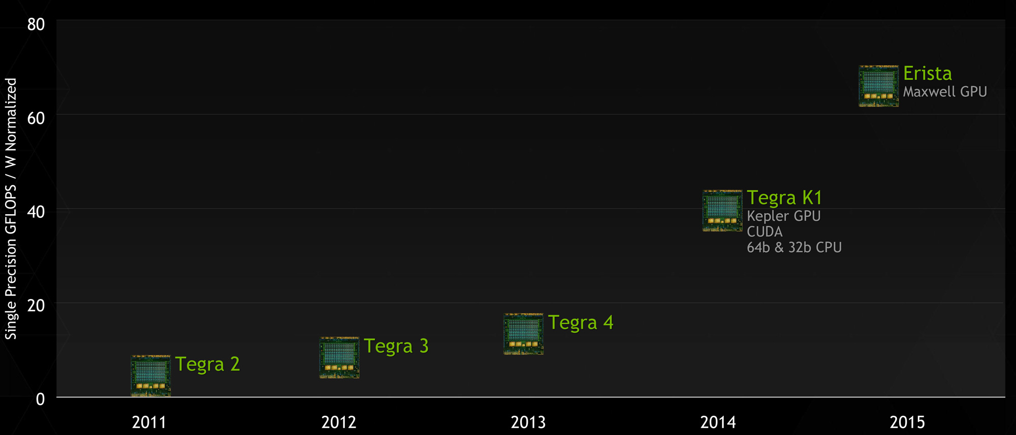
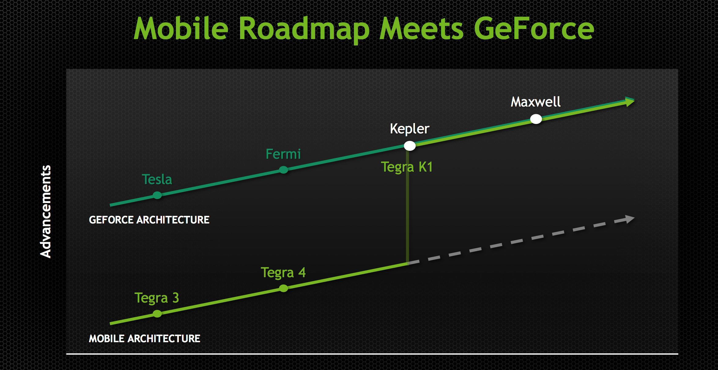
NVIDIA's GTC 2014 Tegra Roadmap
2014 also brought a revision to NVIDIA’s public Tegra roadmap: for 2015 NVIDIA would bump the previously announced Parker SoC and release a new in its place, Erista. This schedule change ended up being quite a surprise due to the fact that NVIDIA had up until this time released their roadmaps roughly 2 years out, whereas Erista was put on the map less than a year before it was to be announced. More unusual, NVIDIA offered up minimal details of Erista; it would be powered by a Maxwell GPU with no additional information on the CPU or manufacturing process. Parker on the other hand – NVIDIA’s planned Denver + Maxwell + 16nm FinFet part – fell off the schedule, with NVIDIA not officially canceling it but also saying little else about it.
Now in 2015 and with the launch of the Tegra X1, we can finally begin putting the picture together. Erista as it turns out is something of a rapid release product for NVIDIA; what had been plans to produce a 16nm FF part in 2015 became plans to produce a 20nm part, with Erista to be that part. To pull together Erista NVIDIA would go for a quick time-to-market approach in SoC design, pairing up a Maxwell GPU with ARM Cortex A57 & A53 GPUs, to be produced on TSMC’s 20nm SoC process.
CPU
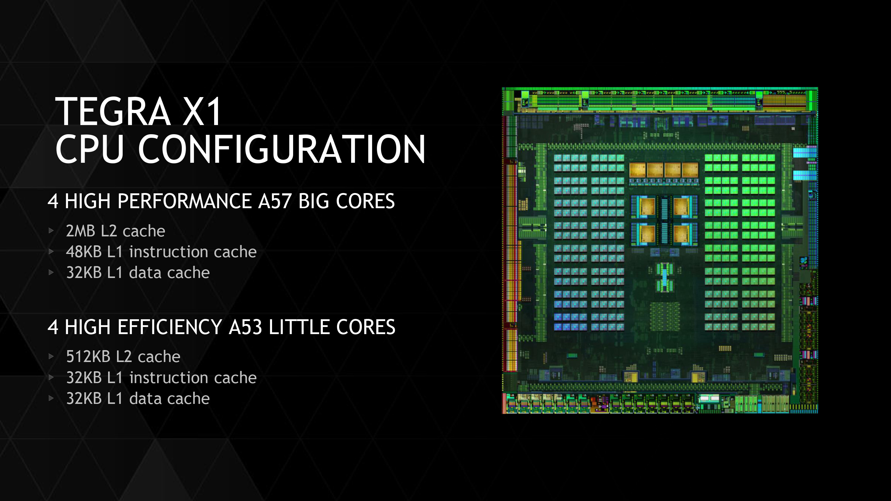
We’ll kick off our look at Erista then with a look at Erista’s CPUs, where one of the bigger surprises in Erista is the CPU configuration. While Tegra K1 had a version with NVIDIA’s custom Denver core for the CPU, NVIDIA has elected to use ARM’s Cortex A57 and A53 in the Tegra X1. The A57 CPU cluster has 2MB of L2 cache shared across the four cores, with 48KB/32KB L1s (I$+D$) per core. The A53 cluster has 512KB of L2 cache shared by all four cores and 32KB/32KB L1s (I$+D$) per core. NVIDIA representatives stated that this was done for time to market reasons.
However, rather than a somewhat standard big.LITTLE configuration as one might expect, NVIDIA continues to use their own unique system. This includes a custom interconnect rather than ARM’s CCI-400, and cluster migration rather than global task scheduling which exposes all eight cores to userspace applications. It’s important to note that NVIDIA’s solution is cache coherent, so this system won't suffer from the power/performance penalties that one might expect given experience with previous SoCs that use cluster migration.
Although cluster migration is usually a detriment to power and performance (especially without a cache coherent interconnect), NVIDIA claims that Tegra X1 significantly outperforms Samsung System LSI’s Exynos 5433 in performance per watt with 1.4x more performance at the same amount of power or half the power for the same performance on the CPU. It's likely that this difference comes from optimizing the implemented logic and differences between Samsung and TSMC 20nm processes rather than differences in thread management. NVIDIA continues to use System EDP (Electrical Design Point) management to control throttling and turbo rather than ARM's IPA (Intelligent Power Allocation) drivers, and in general it seems that while the CPU architecture is ARM's reference design it's quite clear that everything else is distinctly NVIDIA in design.
All of this of course raises the question of where’s Denver, and what is to happen to it? The use of the ARM Cortex A57 and A53, as NVIDIA tells it, was based on a time-to-market decision, and that NVIDIA could bring an off-the-shelf Cortex-based SoC to the market sooner than they could another Denver SoC. On the surface there is at least some evidence to agree with this, as NVIDIA would be able to buy a 20nm design from ARM versus spending the time porting Denver over from TSMC’s 28nm process to their 20nm process. At the same time however integrating an ARM CPU core into an SoC is not an easy task – logic LEGO this is not – so it’s hard to say whether this actually saved NVIDIA much time.
In any case, much like the still in the dark Parker design, NVIDIA is holding their cards close to their chest and hinting that Denver will still be in future generation products. If Parker is still part of NVIDIA’s plans – and they are without a doubt working on some kind of 16nm FF Tegra SoC – then we may still see Denver as part of the original Parker plan. Otherwise at this point while there’s no reason not to believe NVIDIA about the fate of future Denver SoCs, it’s anyone’s guess when we might see it again.
Uncore

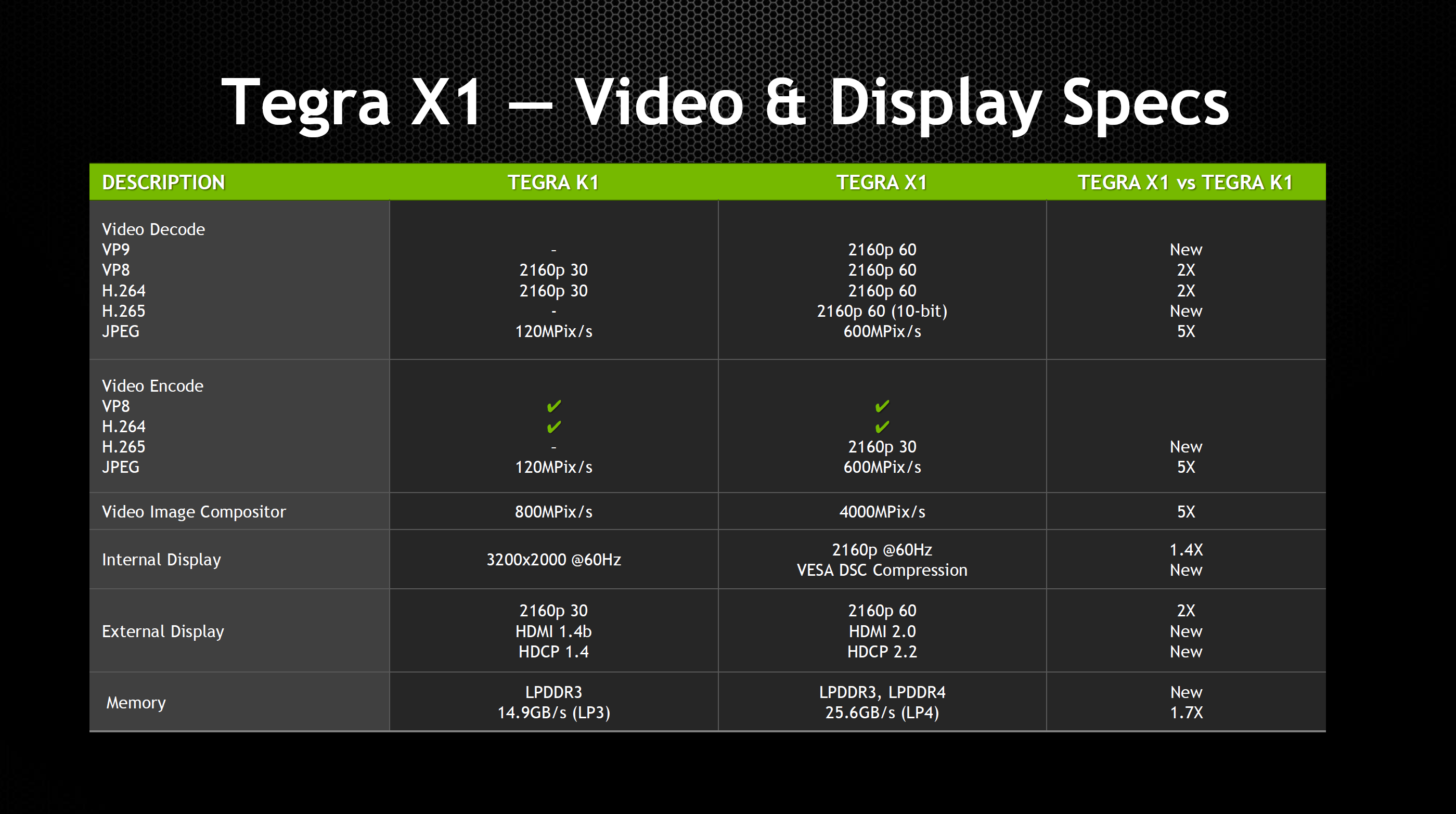
Outside of the CPU and GPU, NVIDIA has also dramatically improved the rest of Tegra X1 in comparison with Tegra K1. We see a move from 64-bit wide LPDDR3 to 64-bit wide LPDDR4 on the memory interface, which improves peak memory bandwidth from 14.9 GB/s to 25.6 GB/s and improves power efficiency by around 40%. In addition, the maximum internal display resolution moves from 3200x2000 at 60 Hz to 3840x2160 at 60 Hz with support for VESA’s display stream compression. For external displays, we see a significant improvement with support for HDMI 2.0 and HDCP 2.2, which means that 4K60 is supported in contrast with the Tegra K1, which only supported 4K30.
The ISP is largely similar to the one we see in the Tegra K1 when it comes to feature set, but JPEG encode and decode rate is now five times as fast, going from 120 MP/s to 600 MP/s. For video encode and decode, we see support for 4K60 H.265 and VP9, with support for 10 bit color on decode on H.265. In addition to support for new codecs in the hardware blocks, we see that H.264 and VP8 now support 4K60, a notable improvement over the 4K30 that was the maximum for Tegra K1. We also see that the storage controller now supports eMMC 5.1 for faster storage performance.
Tegra X1's GPU: Maxwell for Mobile
Going into today’s announcement of the Tegra X1, while NVIDIA’s choice of CPU had been something of a wildcard, the GPU was a known variable. As announced back at GTC 2014, Erista – which we now know as Tegra X1 – would be a future Tegra product with a Maxwell GPU.
Maxwell of course already launched on the PC desktop as a discrete GPU last year in the Maxwell 1 based GM107 and Maxwell 2 based GM204. However despite this otherwise typical GPU launch sequence, Maxwell marks a significant shift in GPU development for NVIDIA that is only now coming to completion with the launch of the X1. Starting with Maxwell, NVIDIA has embarked on a “mobile first” design strategy for their GPUs; unlike Tegra K1 and its Kepler GPU, Maxwell was designed for Tegra from the start rather than being ported after the fact.
By going mobile-first NVIDIA has been able to reap a few benefits. On the Tegra side in particular, mobile-first means that NVIDIA’s latest and greatest GPUs are appearing in SoCs earlier than ever before – the gap between Maxwell 1 and Tegra X1 is only roughly a year, versus nearly two years for Kepler in Tegra K1. But it also means that NVIDIA is integrating deep power optimizations into their GPU architectures at an earlier stage, which for their desktop GPUs has resulted chart-topping power efficiency, and these benefits are meant to cascade down to Tegra as well.
Tegra X1 then is the first SoC to be developed under this new strategy, and for NVIDIA this is a very big deal. From a feature standpoint NVIDIA gets to further build on their already impressive K1 feature set with some of Maxwell’s new features, and meanwhile from a power standpoint NVIDIA wants to build the best A57 SoC on the market. With everyone else implementing (roughly) the same CPU, the GPU stands to be a differentiator and this is where NVIDIA believes their GPU expertise translates into a significant advantage.
Diving into the X1’s GPU then, what we have is a Tegra-focused version of Maxwell 2. Compared to Kepler before it, Maxwell 2 introduced a slew of new features into the NVIDIA GPU architecture, including 3rd generation delta color compression, streamlined SMMs with greater efficiency per CUDA core, and graphics features such as conservative rasterization, volumetric tiled resources, and multi-frame anti-aliasing. All of these features are making their way into Tegra X1, and for brevity’s sake rather than rehashing all of this we’ll defer to our deep dive on the Maxwell 2 architecture from the launch of the GeForce GTX 980.
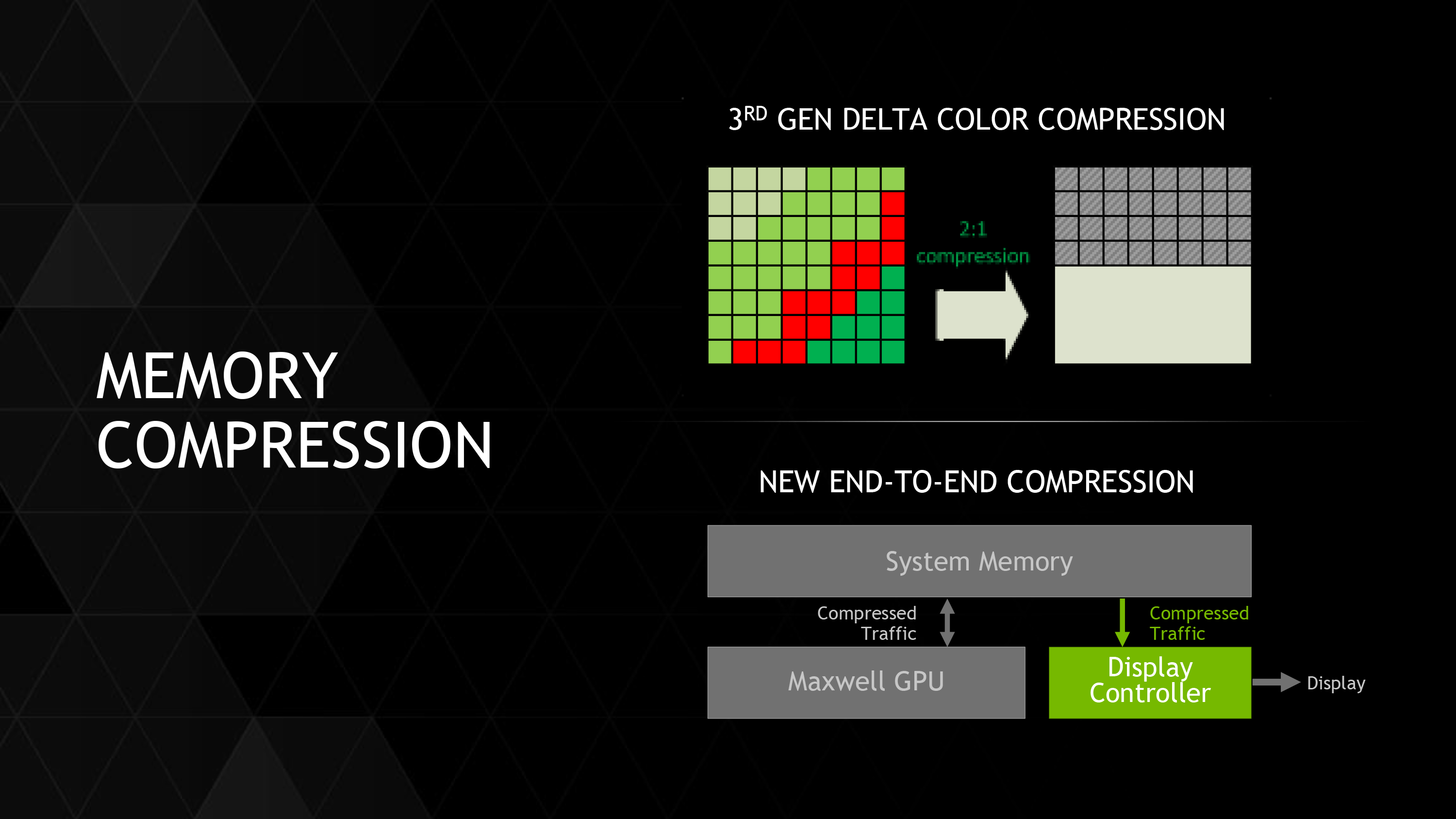
For X1 in particular, while every element helps, NVIDIA’s memory bandwidth and overall efficiency increases are going to be among the most important of these improvements since they address two of the biggest performance bottlenecks facing SoC-class GPUs. In the case of memory bandwidth optimizations, memory bandwidth has long been a bottleneck at higher performance levels and resolutions, and while it’s a solvable problem, the general solution is to build a wider (96-bit or 128-bit) memory bus, which is very effective but also drives up the cost and complexity of the SoC and the supporting hardware. In this case NVIDIA is sticking to a 64-bit memory bus, so memory compression is very important for NVIDIA to help drive X1. This coupled with a generous increase in memory bandwidth from the move to LPDDR4 helps to ensure that X1’s more powerful GPU won’t immediately get starved at the memory stage.
Meanwhile just about everything about SoC TDP that can be said has been said. TDP is a limiting factor in all modern mobile devices, which means deceased power consumption directly translates into increased performance, especially under sustained loads. Coupled with TSMC’s 20nm SoC process, Maxwell’s power optimizations will further improve NVIDIA’s SoC GPU performance.
Double Speed FP16
Last but certainly not least however, X1 will also be launching with a new mobile-centric GPU feature not found on desktop Maxwell. For X1 NVIDIA is implanting what they call “double speed FP16” support in their CUDA cores, which is to say that they are implementing support for higher performance FP16 operations in limited circumstances.
As with Kepler and Fermi before it, Maxwell only features dedicated FP32 and FP64 CUDA cores, and this is still the same for X1. However in recognition of how important FP16 performance is, NVIDIA is changing how they are handling FP16 operations for X1. On K1 FP16 operations were simply promoted to FP32 operations and run on the FP32 CUDA cores; but for X1, FP16 operations can in certain cases be packed together as a single Vec2 and issued over a single FP32 CUDA core.
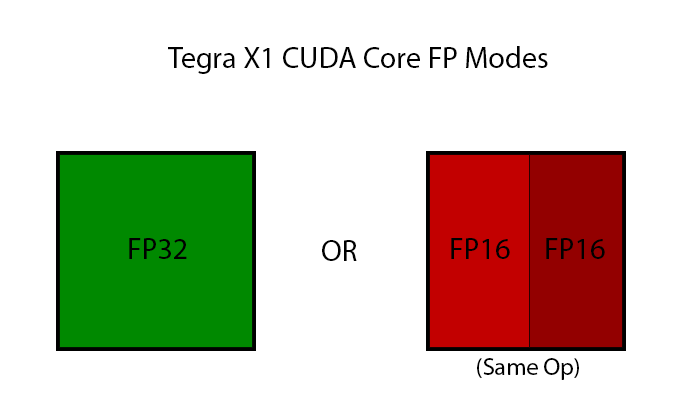
There are several special cases here, but in a nutshell NVIDIA can pack together FP16 operations as long as they’re the same operation, e.g. both FP16s are undergoing addition, multiplication, etc. Fused multiply-add (FMA/MADD) is also a supported operation here, which is important for how frequently it is used and is necessary to extract the maximum throughput out of the CUDA cores.
In this respect NVIDIA is playing a bit of catch up to the competition, and overall it’s hard to escape the fact that this solution is a bit hack-ish, but credit where credit is due to NVIDIA for at least recognizing and responding to what their competition has been doing. Both ARM and Imagination have FP16 capabilities on their current generation parts (be it dedicated FP16 units or better ALU decomposition), and even AMD is going this route for GCN 1.2. So even if it only works for a few types of operations, this should help ensure NVIDIA doesn’t run past the competition on FP32 only to fall behind on FP16.
So why are FP16 operations so important? The short answer is for a few reasons. FP16 operations are heavily used in Android’s display compositor due to the simplistic (low-precision) nature of the work and the power savings, and FP16 operations are also used in mobile games at certain points. More critical to NVIDIA’s goals however, FP16 can also be leveraged for computer vision applications such as image recognition, which NVIDIA needs for their DRIVE PX platform (more on that later). In both of these cases FP16 does present its own limitations – 16-bits just isn’t very many bits to hold a floating point number – but there are enough cases where it’s still precise enough that it’s worth the time and effort to build in the ability to process it quickly.
Tegra X1 GPU By The Numbers
Now that we’ve covered the X1’s GPU from a feature perspective, let’s take a look the GPU from a functional unit/specification perspective.
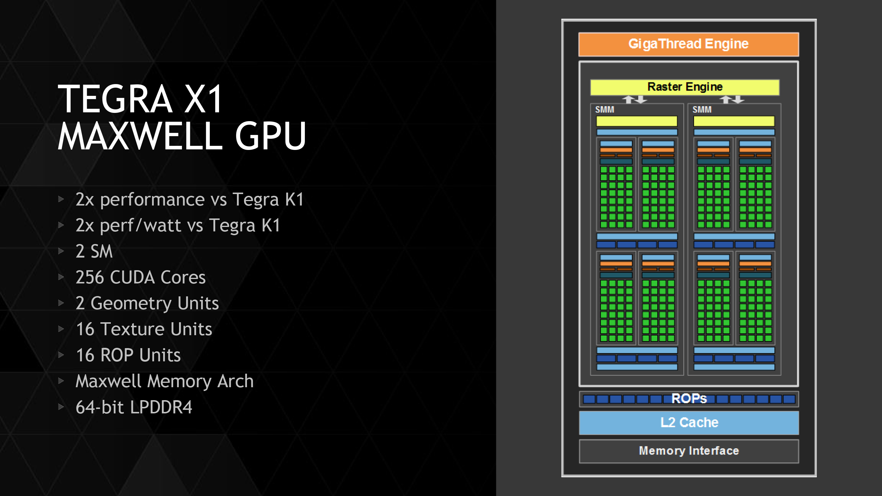
Overall the X1’s GPU is composed of 2 Maxwell SMMs inside a single GPC, for a total of 256 CUDA cores. This compares very favorably to the single SMX in K1, as it means certain per-SMM/SMX resources such as the geometry and texture units have been doubled. Furthermore Maxwell’s more efficient CUDA cores means that X1 is capable of further extending its lead over Kepler, as we’ve already seen in the desktop space.
| NVIDIA Tegra GPU Specification Comparison | ||||
| K1 | X1 | |||
| CUDA Cores | 192 | 256 | ||
| Texture Units | 8 | 16 | ||
| ROPs | 4 | 16 | ||
| GPU Clock | ~950MHz | ~1000MHz | ||
| Memory Clock | 930MHz (LPDDR3) | 1600MHz (LPDDR4) | ||
| Memory Bus Width | 64-bit | 64-bit | ||
| FP16 Peak | 365 GFLOPS | 1024 GFLOPS | ||
| FP32 Peak | 365 GFLOPS | 512 GFLOPS | ||
| Architecture | Kepler | Maxwell | ||
| Manufacturing Process | TSMC 28nm | TSMC 20nm SoC | ||
Meanwhile outside of the CUDA cores NVIDIA has also made an interesting move in X1’s ROP configuration. At 16 ROPs the X1 has four times the ROPs of K1, and is consequently comparatively ROP heavy. This is as many ROPs as is on a GM107 GPU, for example. With that said, due to NVIDIA’s overall performance goals and their desire to drive 4K displays at 60Hz, there is a definite need to go ROP-heavy to make sure they can push the necessary amount of pixels. This also goes hand-in-hand with NVIDIA’s memory bandwidth improvements (efficiency and actual) which will make it much easier to feed those ROPs. This also puts the ROP:memory controller ratio at 16:1, the same ratio as on NVIDIA’s desktop Maxwell parts.
Finally, let’s talk about clockspeeds and expected performance. While NVIDIA is not officially publishing the GPU clockspeeds for the X1, based on their performance figures it’s easy to figure out. With NVIDIA’s quoted (and promoted) 1 TFLOPs FP16 performance figure for the X1, the clockspeed works out to a full 1GHz for the GPU (1GHz * 2 FP 16 * 2 FMA * 256 = 1 TFLOPs).
This is basically a desktop-class clockspeed, and it goes without saying that is a very aggressive GPU clockspeed for an SoC-class part. We’re going to have to see what design wins X1 lands and what the devices are like, but right now it’s reasonable to expect that mobile devices will only burst here for short periods of time at best. However NVIDIA’s fixed platform DRIVE devices are another story; those can conceivably be powered and cooled well enough that the X1’s GPU can hit and sustain these clockspeeds.
GPU Performance Benchmarks
As part of today’s announcement of the Tegra X1, NVIDIA also gave us a short opportunity to benchmark the X1 reference platform under controlled circumstances. In this case NVIDIA had several reference platforms plugged in and running, pre-loaded with various benchmark applications. The reference platforms themselves had a simple heatspreader mounted on them, intended to replicate the ~5W heat dissipation capabilities of a tablet.
The purpose of this demonstration was two-fold. First to showcase that X1 was up and running and capable of NVIDIA’s promised features. The second reason was to showcase the strong GPU performance of the platform. Meanwhile NVIDIA also had an iPad Air 2 on hand for power testing, running Apple’s latest and greatest SoC, the A8X. NVIDIA has made it clear that they consider Apple the SoC manufacturer to beat right now, as A8X’s PowerVR GX6850 GPU is the fastest among the currently shipping SoCs.
It goes without saying that the results should be taken with an appropriate grain of salt until we can get Tegra X1 back to our labs. However we have seen all of the testing first-hand and as best as we can tell NVIDIA’s tests were sincere.
| NVIDIA Tegra X1 Controlled Benchmarks | |||||
| Benchmark | A8X (AT) | K1 (AT) | X1 (NV) | ||
| BaseMark X 1.1 Dunes (Offscreen) | 40.2fps | 36.3fps | 56.9fps | ||
| 3DMark 1.2 Unlimited (Graphics Score) | 31781 | 36688 | 58448 | ||
| GFXBench 3.0 Manhattan 1080p (Offscreen) | 32.6fps | 31.7fps | 63.6fps | ||
For benchmarking NVIDIA had BaseMark X 1.1, 3DMark Unlimited 1.2 and GFXBench 3.0 up and running. Our X1 numbers come from the benchmarks we ran as part of NVIDIA’s controlled test, meanwhile the A8X and K1 numbers come from our Mobile Bench.
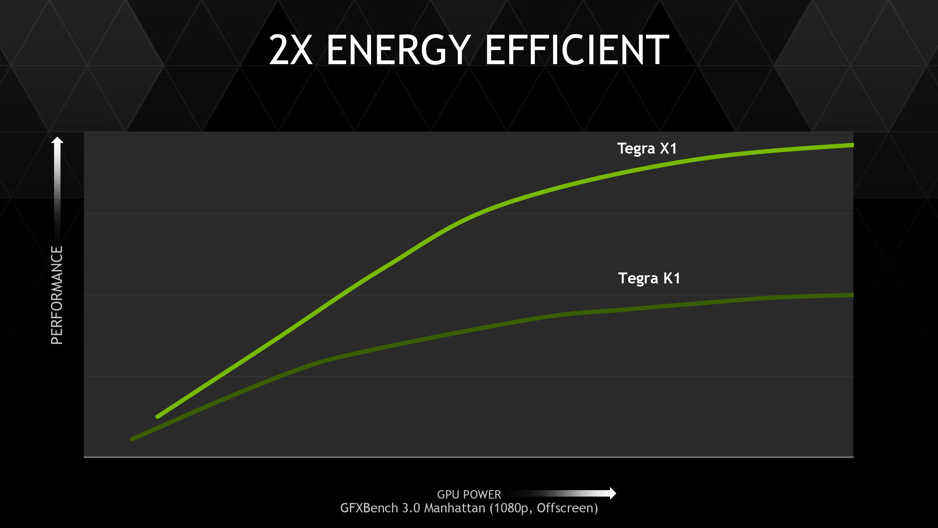
NVIDIA’s stated goal with X1 is to (roughly) double K1’s GPU performance, and while these controlled benchmarks for the most part don’t make it quite that far, X1 is still a significant improvement over K1. NVIDIA does meet their goal under Manhattan, where performance is almost exactly doubled, meanwhile 3DMark and BaseMark X increased by 59% and 56% respectively.
Finally, for power testing NVIDIA had an X1 reference platform and an iPad Air 2 rigged to measure the power consumption from the devices’ respective GPU power rails. The purpose of this test was to showcase that thanks to X1’s energy optimizations that X1 is capable of delivering the same GPU performance as the A8X GPU while drawing significantly less power; in other words that X1’s GPU is more efficient than A8X’s GX6850. Now to be clear here these are just GPU power measurements and not total platform power measurements, so this won’t account for CPU differences (e.g. A57 versus Enhanced Cyclone) or the power impact of LPDDR4.
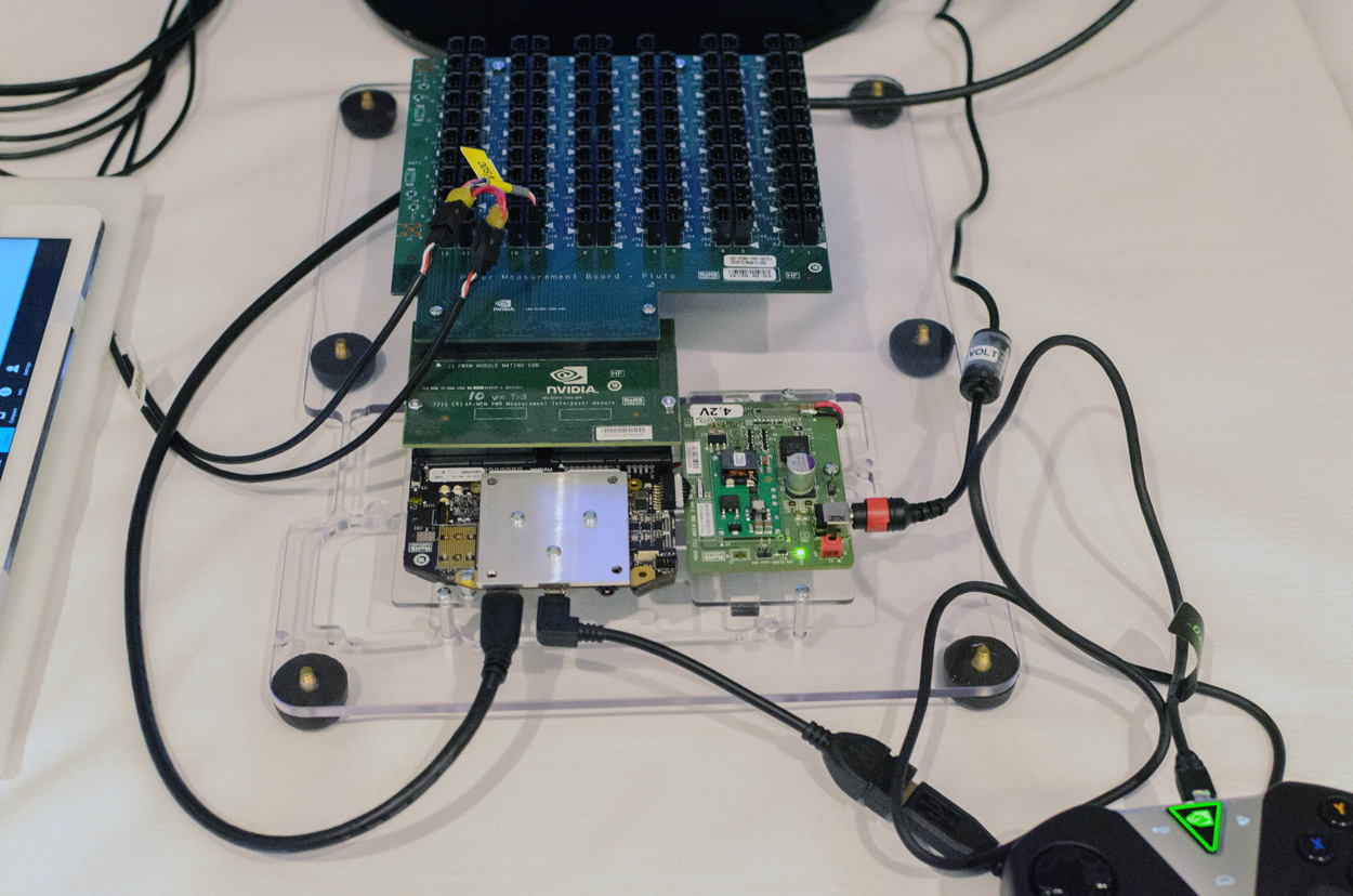
Top: Tegra X1 Reference Platform. Bottom: iPad Air 2
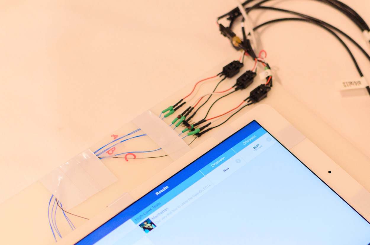
For power testing NVIDIA ran Manhattan 1080p (offscreen) with X1’s GPU underclocked to match the performance of the A8X at roughly 33fps. Pictured below are the average power consumption (in watts) for the X1 and A8X respectively.
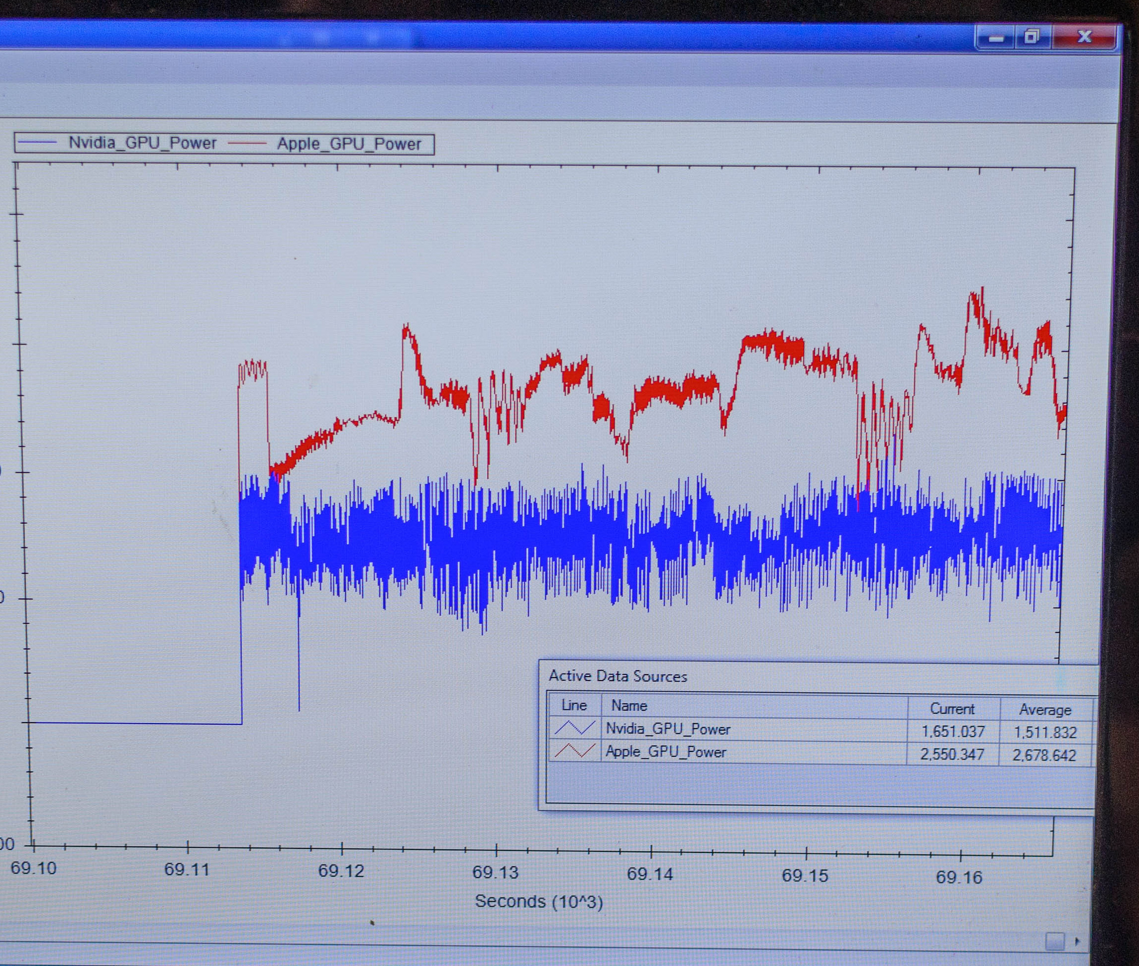

NVIDIA’s tools show the X1’s GPU averages 1.51W over the run of Manhattan. Meanwhile the A8X’s GPU averages 2.67W, over a watt more for otherwise equal performance. This test is especially notable since both SoCs are manufactured on the same TSMC 20nm SoC process, which means that any performance differences between the two devices are solely a function of energy efficiency.
There are a number of other variables we’ll ultimately need to take into account here, including clockspeeds, relative die area of the GPU, and total platform power consumption. But assuming NVIDIA’s numbers hold up in final devices, X1’s GPU is looking very good out of the gate – at least when tuned for power over performance.
Automotive: DRIVE CX and DRIVE PX
While NVIDIA has been a GPU company throughout the entire history of the company, they will be the first to tell you that they know they can’t remain strictly a GPU company forever, and that they must diversify themselves if they are to survive over the long run. The result of this need has been a focus by NVIDIA over the last half-decade or so on offering a wider range of hardware and even software. Tegra SoCs in turn have been a big part of that plan so far, but NVIDIA of recent years has become increasingly discontent as a pure hardware provider, leading to the company branching out in unusual ways and not just focusing on selling hardware, but selling buyers on whole solutions or experiences. GRID, Gameworks, and NVIDIA’s Visual Computing Appliances have all be part of this branching out process.
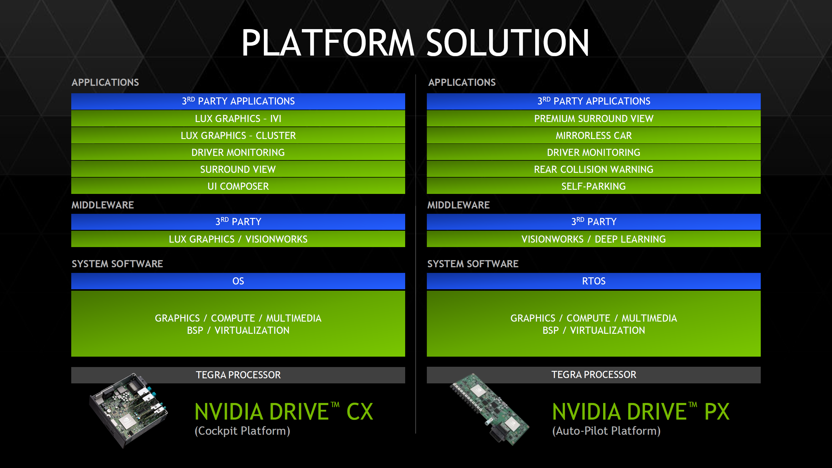
Meanwhile with unabashed car enthusiast Jen-Hsun Huang at the helm of NVIDIA, it’s slightly less than coincidental that the company has also been branching out in to automotive technology as well. Though still an early field for NVIDIA, the company’s Tegra sales for automotive purposes have otherwise been a bright spot in the larger struggles Tegra has faced. And now amidst the backdrop of CES 2015 the company is taking their next step into automotive technology by expanding beyond just selling Tegras to automobile manufacturers, and into selling manufacturers complete automotive solutions. To this end, NVIDIA is announcing two new automotive platforms, NVIDIA DRIVE CX and DRIVE PX.
DRIVE CX is NVIDIA’s in-car computing platform, which is designed to power in-car entertainment, navigation, and instrument clusters. While it may seem a bit odd to use a mobile SoC for such an application, Tesla Motors has shown that this is more than viable.
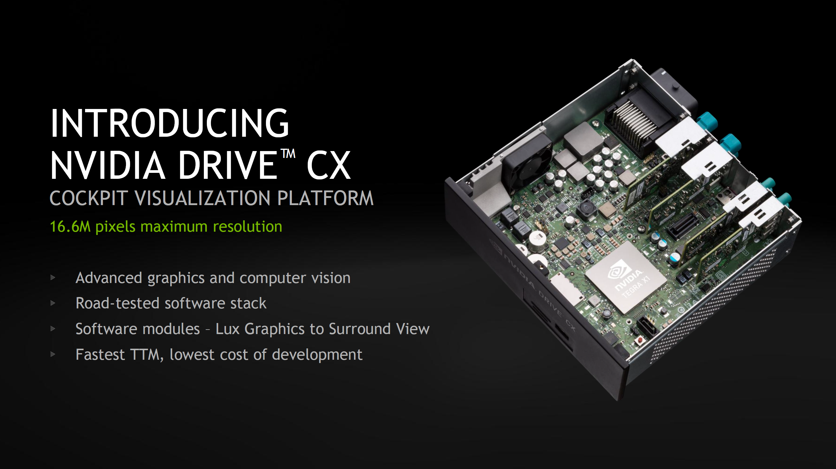
With NVIDIA’s DRIVE CX, automotive OEMs have a Tegra X1 in a board that provides support for Bluetooth, modems, audio systems, cameras, and other interfaces needed to integrate such an SoC into a car. This makes it possible to drive up to 16.6MP of display resolution, which would be around two 4K displays or eight 1080p displays. However, each DRIVE CX module can only drive three displays. In press photos, it appears that this platform also has a fan which is likely necessary to enable Tegra X1 to run continuously at maximum performance without throttling.
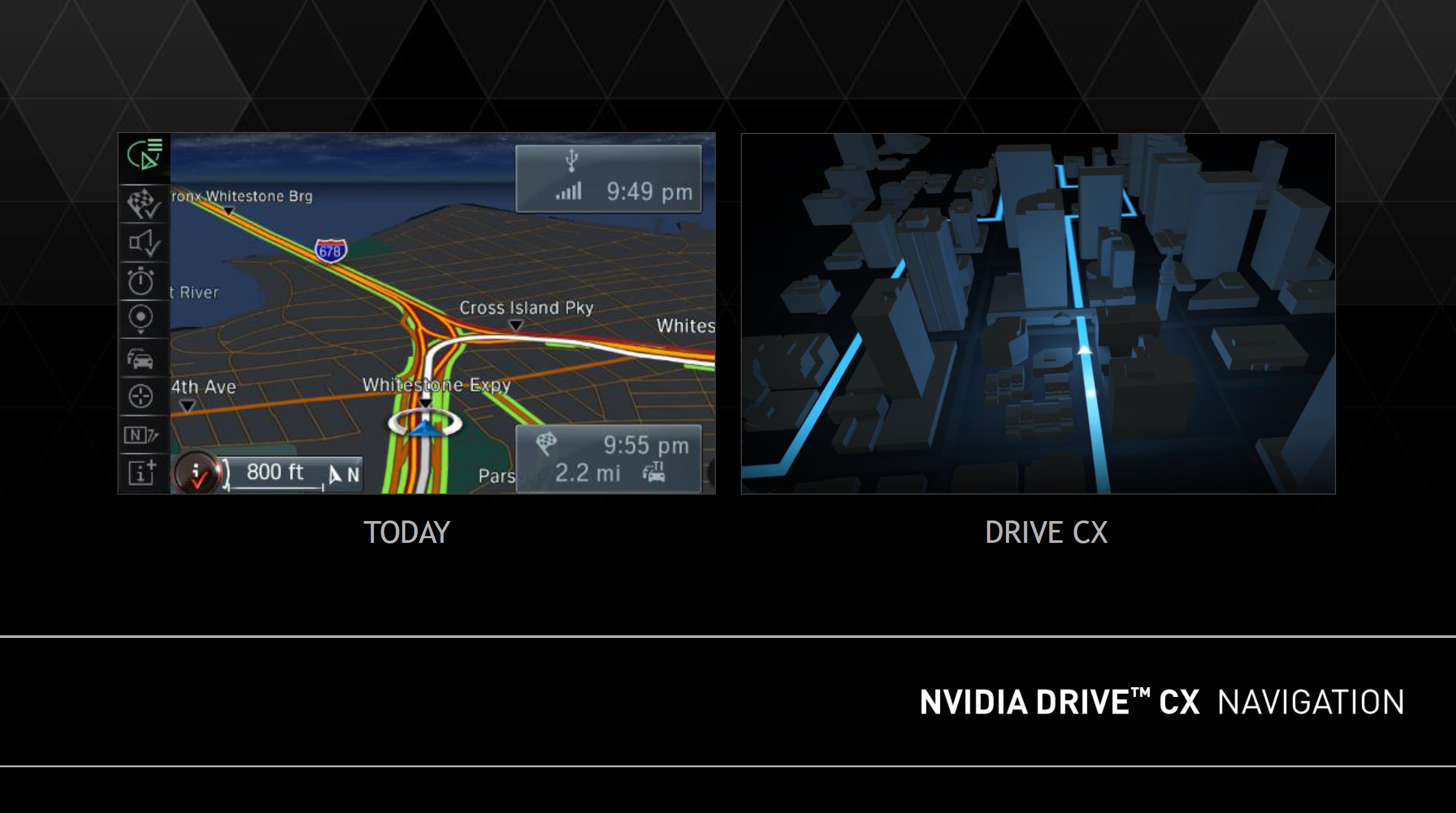
NVIDIA showed off some examples of where DRIVE CX would improve over existing car computing systems in the form of advanced 3D rendering for navigation to better convey information, and 3D instrument clusters which are said to better match cars with premium design. Although the latter is a bit gimmicky, it does seem like DRIVE CX has a strong selling point in the form of providing an in-car computing platform with a large amount of compute while driving down the time and cost spent developing such a platform.
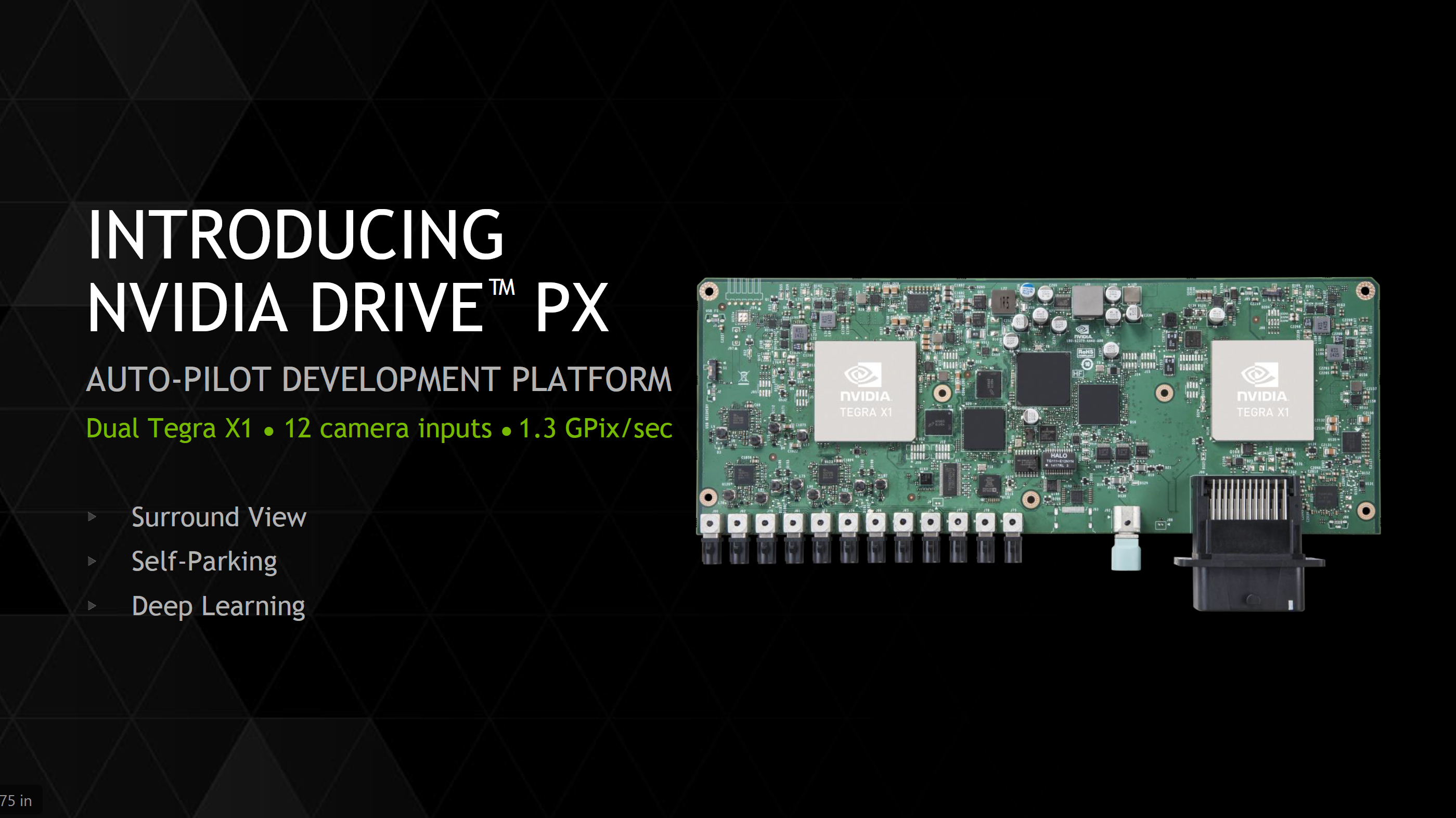
While DRIVE CX seems to be a logical application of a mobile SoC, DRIVE PX puts mobile SoCs in car autopilot applications. To do this, the DRIVE PX platform uses two Tegra X1 SoCs to support up to twelve cameras with aggregate bandwidth of 1300 megapixels per second. This means that it’s possible to have all twelve cameras capturing 1080p video at around 60 FPS or 720p video at 120 FPS. NVIDIA has also made most of the software stack needed for autopilot applications already, so there would be comparatively much less time and cost needed to implement features such as surround vision, auto-valet parking, and advanced driver assistance.
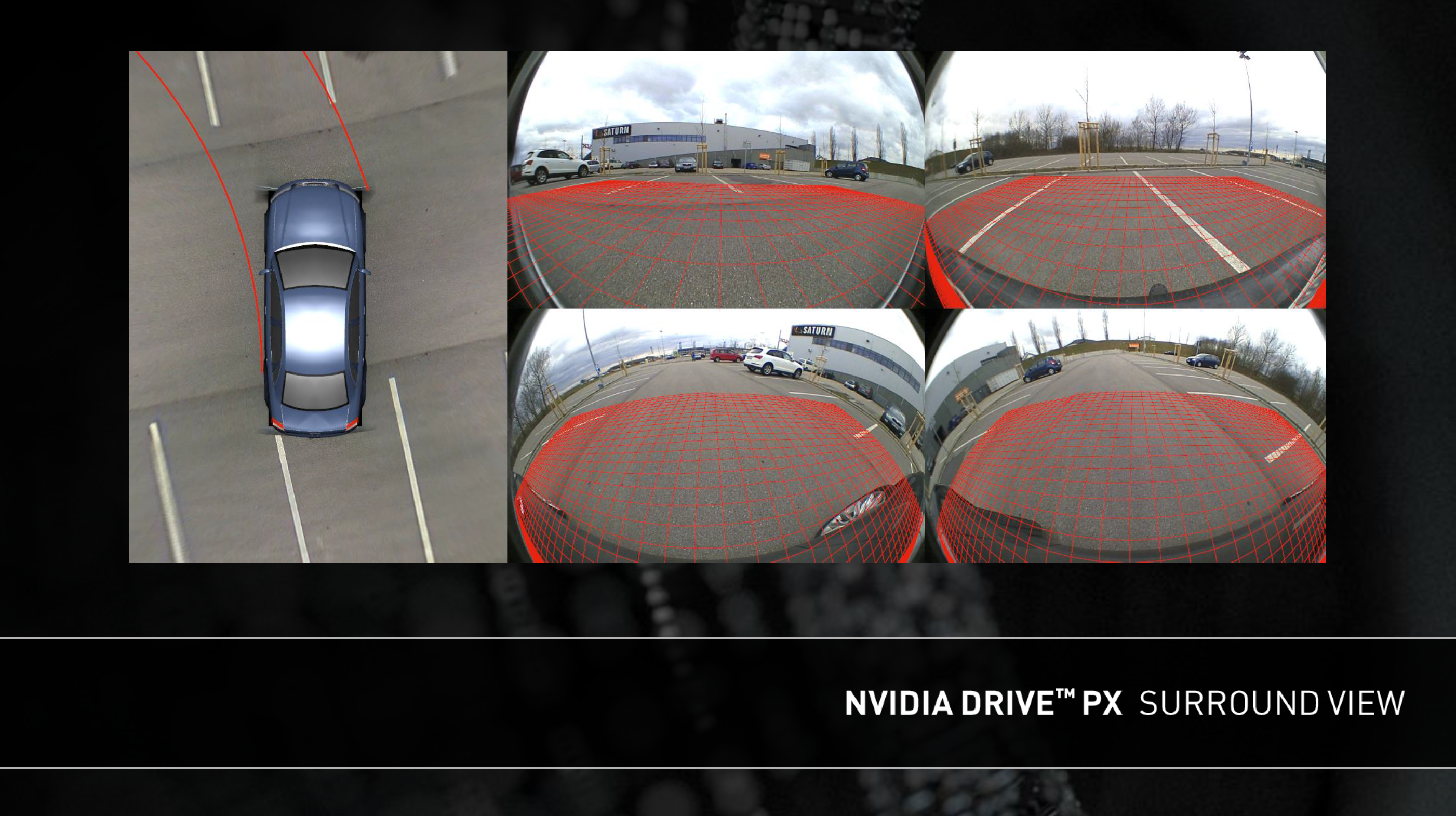
In the case of surround vision, DRIVE PX is said to deliver a better experience by improving stitching of video to reduce visual artifacts and compensate for varying lighting conditions.
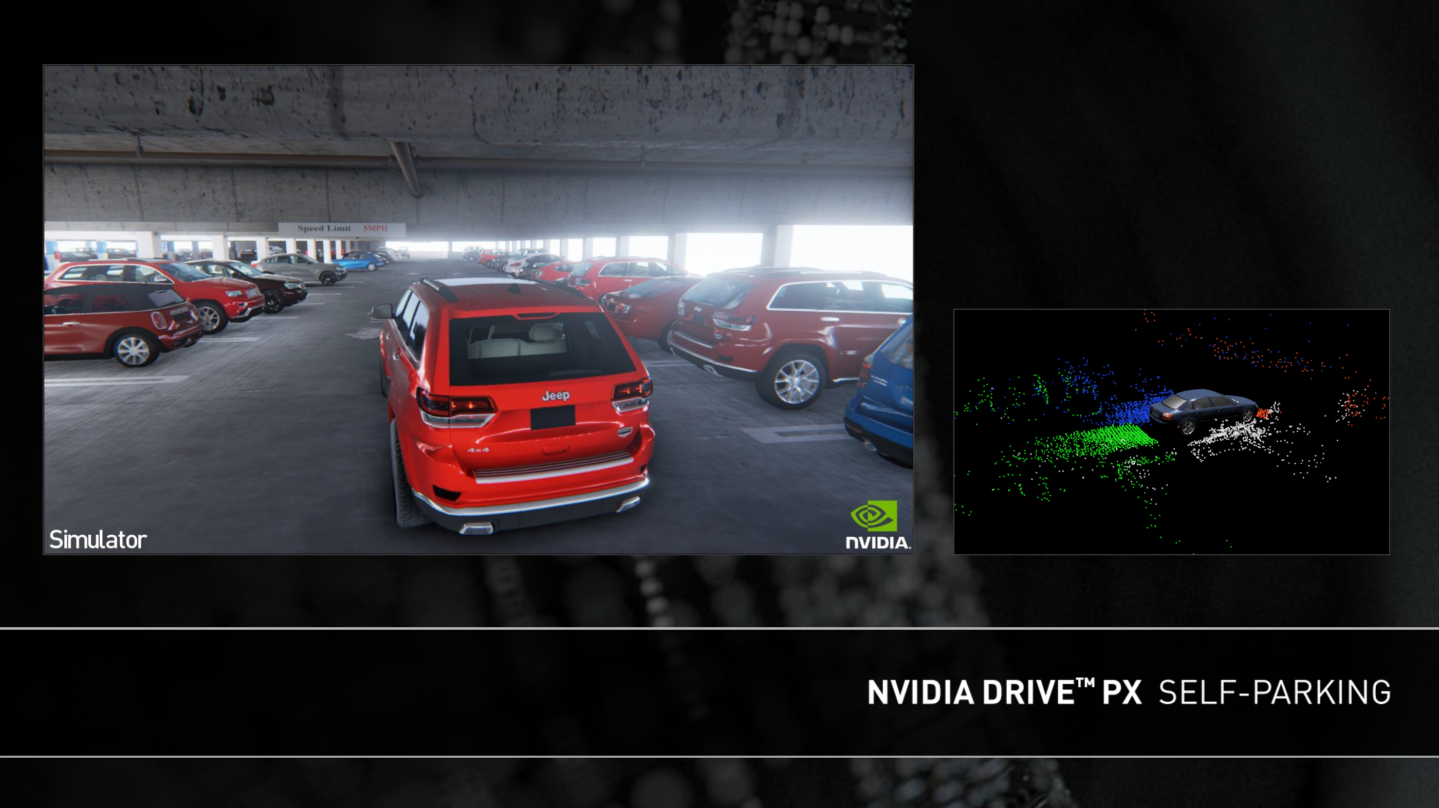
The valet parking feature seems to build upon this surround vision system, as it uses cameras to build a 3D representation of the parking lot along with feature detection to drive through a garage looking for a valid parking spot (no handicap logo, parking lines present, etc) and then autonomously parks the car once a valid spot is found.
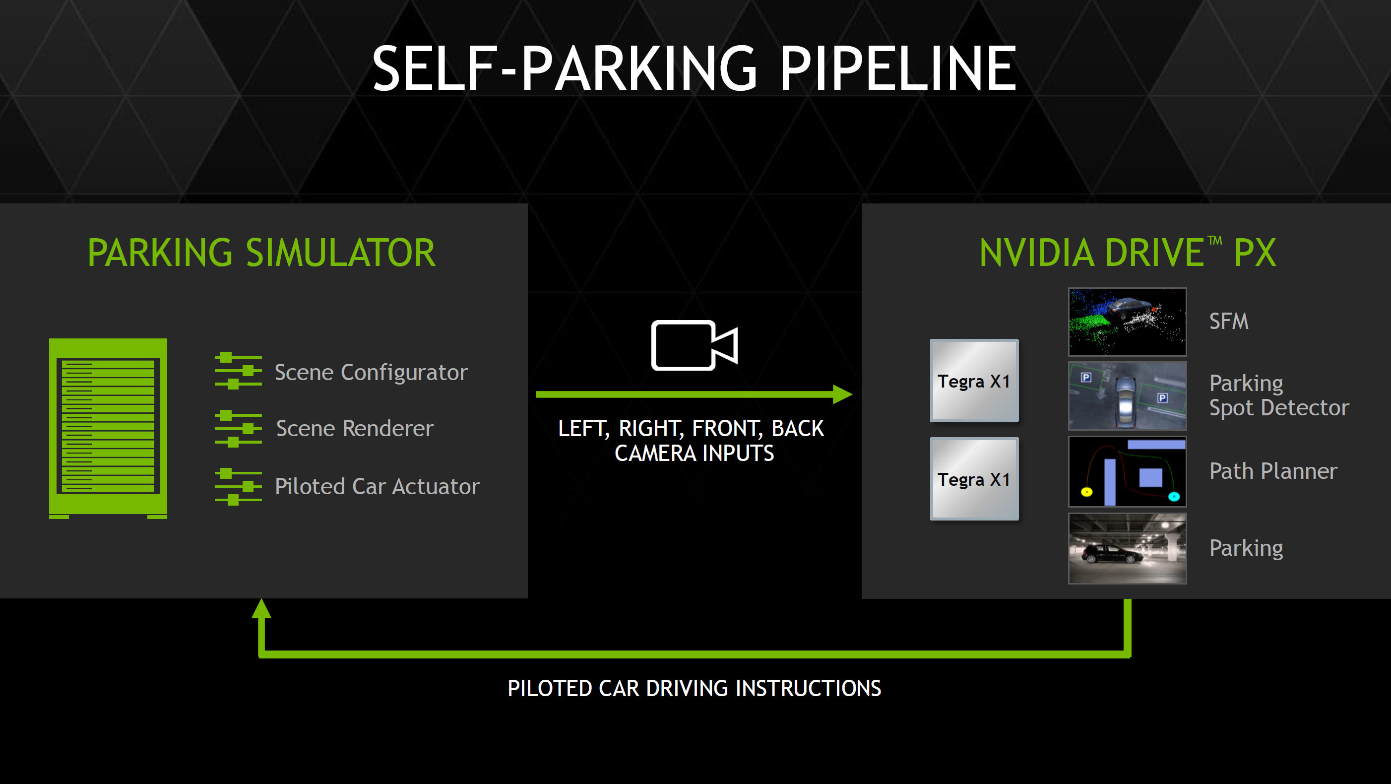
NVIDIA has also developed an auto-valet simulator system with five GTX 980 GPUs to make it possible for OEMs to rapidly develop self-parking algorithms.
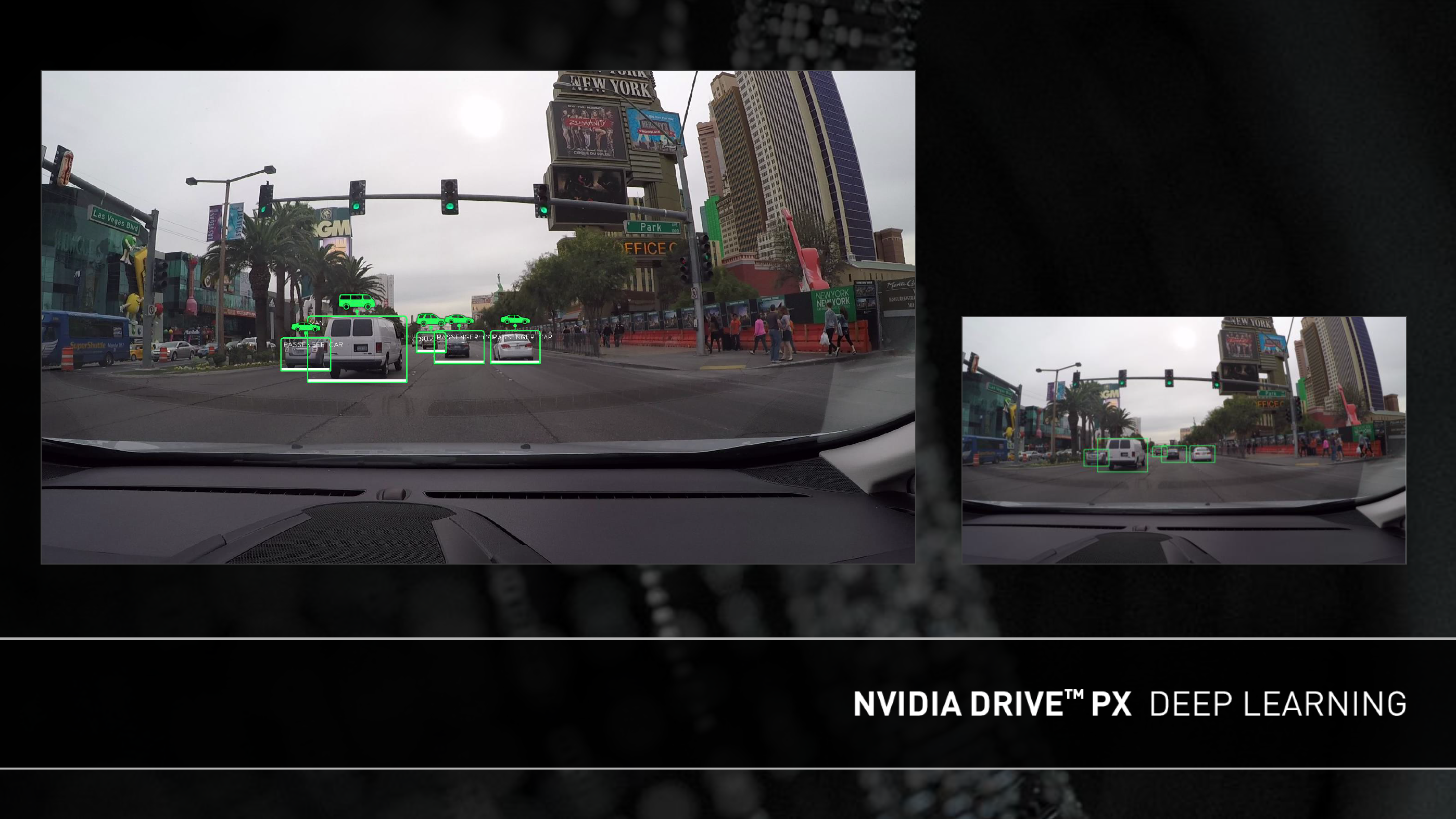
The final feature of DRIVE PX, advanced driver assistance, is possibly the most computationally intensive out of all three of the previously discussed features. In order to deliver a truly useful driver assistance system, NVIDIA has leveraged neural network technologies which allow for object recognition with extremely high accuracy.
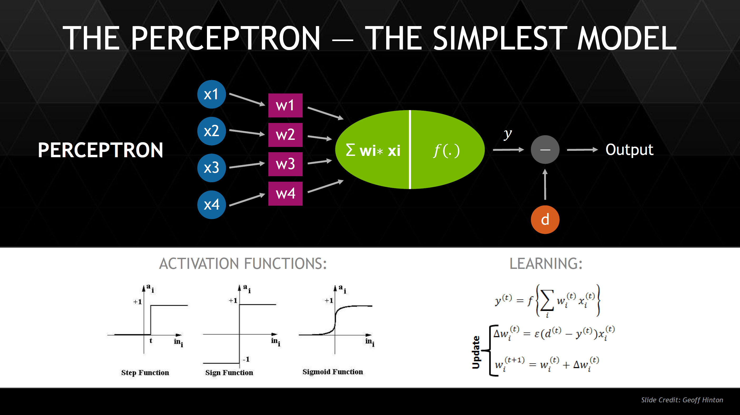
While we won’t dive into deep detail on how such neural networks work, in essence a neural network is composed of perceptrons, which are analogous to neurons. These perceptrons receive various inputs, then given certain stimulus levels for each input the perceptron returns a Boolean (true or false). By combining perceptrons to form a network, it becomes possible to teach a neural network to recognize objects in a useful manner. It’s also important to note that such neural networks are easily parallelized, which means that GPU performance can dramatically improve performance of such neural networks. For example, DRIVE PX would be able to detect if a traffic light is red, whether there is an ambulance with sirens on or off, whether a pedestrian is distracted or aware of traffic, and the content of various road signs. Such neural networks would also be able to detect such objects even if they are occluded by other objects, or if there are differing light conditions or viewpoints.

While honing such a system would take millions of test images to reach high accuracy levels, NVIDIA is leveraging Tesla in the cloud for training neural networks that are then loaded into DRIVE PX instead of local training. In addition, failed identifications are logged and uploaded to the cloud in order to further improve the neural network. Both of these updates can be done either over the air or at service time, which should mean that driver assistance will improve with time. It isn’t a far leap to see how such technology could also be leveraged in self-driving cars as well.
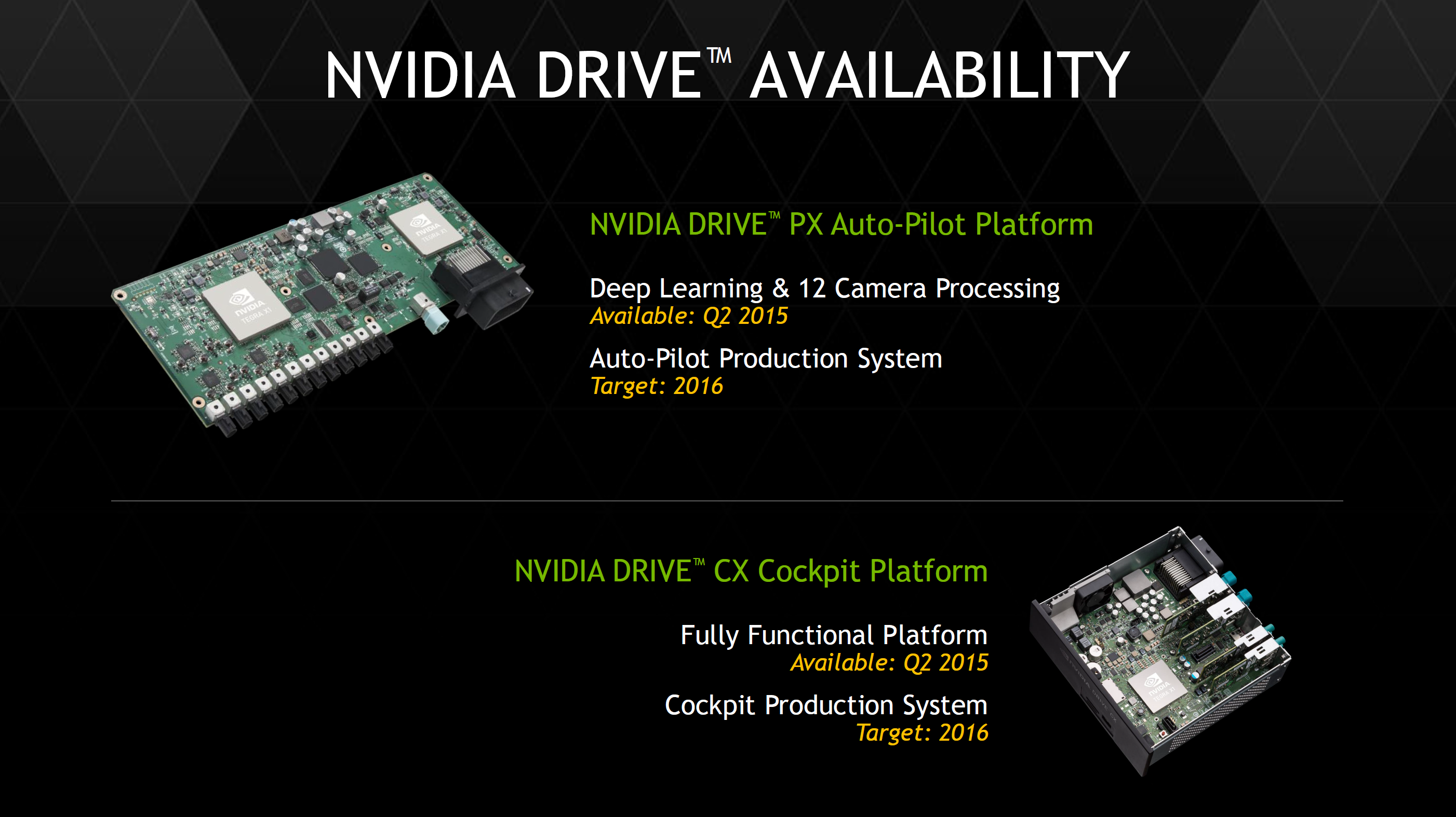
Overall, NVIDIA seems to be planning for the DRIVE platforms to be ready next quarter, and production systems to be ready for 2016. This should mean that it's possible for vehicles launching in 2016 to have some sort of DRIVE system present, although it's possible that it would take until 2017 to see this happen.
Final Words
With the Tegra X1, there have been a great deal of changes when compared to Tegra K1. We see a move from Cortex A15 to A57 on the main cluster, and a move from a single low power Cortex A15 to four Cortex A53s which is a significant departure from previous Tegra SoCs. However, the CPU design remains distinct from what we see in SoCs like the Exynos 5433, as NVIDIA uses a custom CPU interconnect and cluster migration instead of ARM’s CCI-400 and global task scheduling. Outside of these CPU changes, NVIDIA has done a great deal of work on the uncore, with a much faster ISP and support for new codecs at high resolution and frame rate, along with an improved memory interface and improved display output.
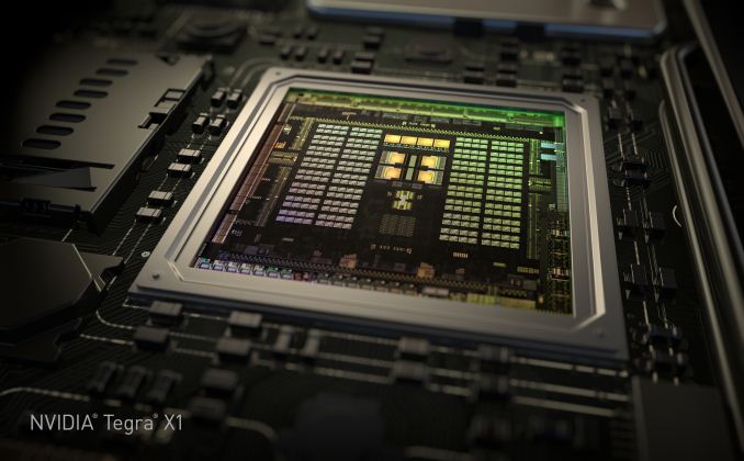
Tegra X1 Reference Platform
Outside of CPU, the GPU is a massive improvement with the move to Maxwell. The addition of double-speed FP16 support for the Tegra X1 helps to improve performance and power efficiency in applications that will utilize FP16, and in general the mobile-first focus on the architecture makes for a 2x improvement in performance per watt. While Tegra K1 set a new bar for mobile graphics for other SoC designers to target, Tegra X1 manages to raise the bar again in a big way. Given the standards support of Tegra X1, it wouldn’t be a far leap to see more extensive porting of games to a version of SHIELD Tablet with Tegra X1.
NVIDIA has also made automotive applications a huge focus in Tegra X1 in the form of DRIVE CX, a cockpit computing platform, and DRIVE PX, an autopilot platform. Given the level of integration and compute present in both DRIVE CX and PX, there seems to be a significant amount of value in NVIDIA’s solutions. However, it remains to be seen whether OEMs will widely adopt these solutions as car manufacturers can take multiple years to implement a new SoC. Compared to the 3-4 month adoption rate of an SoC in a phone or tablet, it's hard to pass any judgment on whether or not NVIDIA's automotive endeavors will be a success.
Overall, Tegra X1 represents a solid improvement over Tegra K1, and now that NVIDIA has shifted their GPU architectures to be targeted at mobile first, we’re seeing the benefits that come with such a strategy. It seems obvious that this would be a great SoC to put in a gaming tablet and a variety of other mobile devices, but it remains to be seen whether NVIDIA can get the design wins necessary to make this happen. Given that all of the high-end SoCs in the Android space will be shipping with A57 and A53 CPUs, the high-end SoC space will see significant competition once again.


