The RV870 Story: AMD Showing up to the Fight
by Anand Lal Shimpi on February 14, 2010 12:00 AM EST- Posted in
- GPUs
The Payoff: How RV740 Saved Cypress
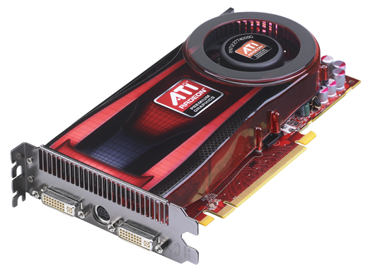
For its first 40nm GPU, ATI chose the biggest die that made sense in its roadmap. That was the RV740 (Radeon HD 4770):

The first to 40nm - The ATI Radeon HD 4770, April 2009
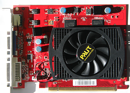
NVIDIA however picked a smaller die. While the RV740 was a 137mm2 GPU, NVIDIA’s first 40nm parts were the G210 and GT220 which measured 57mm2 and 100mm2. The G210 and GT220 were OEM-only for the first months of their life, and I’m guessing the G210 made up a good percentage of those orders. Note that it wasn’t until the release of the GeForce GT 240 that NVIDIA made a 40nm die equal in size to the RV740. The GT 240 came out in November 2009, while the Radeon HD 4770 (RV740) debuted in April 2009 - 7 months earlier.

NVIDIA's first 40nm GPUs shipped in July 2009
When it came time for both ATI and NVIDIA to move their high performance GPUs to 40nm, ATI had more experience and exposure to the big die problems with TSMC’s process.
David Wang, ATI’s VP of Graphics Engineering at the time, had concerns about TSMC’s 40nm process that he voiced to Carrell early on in the RV740 design process. David was worried that the metal handling in the fabrication process might lead to via quality issues. Vias are tiny connections between the different metal layers on a chip, and the thinking was that the via failure rate at 40nm was high enough to impact the yield of the process. Even if the vias wouldn’t fail completely, the quality of the via would degrade the signal going through the via.
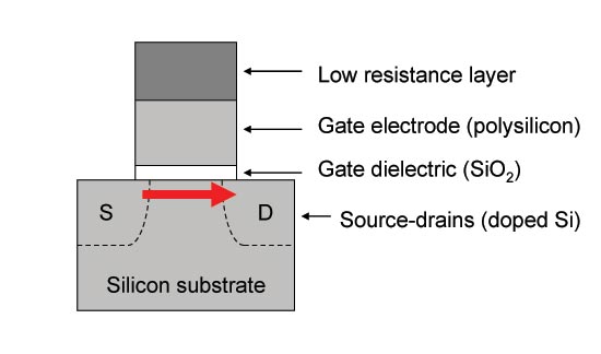
The second cause for concern with TSMC’s 40nm process was about variation in transistor dimensions. There are thousands of dimensions in semiconductor design that you have to worry about. And as with any sort of manufacturing, there’s variance in many if not all of those dimensions from chip to chip. David was particularly worried about manufacturing variation in transistor channel length. He was worried that the tolerances ATI were given might not be met.

A standard CMOS transistor. Its dimensions are usually known to fairly tight tolerances.
TSMC led ATI to believe that the variation in channel length was going to be relatively small. Carrell and crew were nervous, but there’s nothing that could be done.
The problem with vias was easy (but costly) to get around. David Wang decided to double up on vias with the RV740. At any point in the design where there was a via that connected two metal layers, the RV740 called for two. It made the chip bigger, but it’s better than having chips that wouldn’t work. The issue of channel length variation however, had no immediate solution - it was a worry of theirs, but perhaps an irrational fear.
TSMC went off to fab the initial RV740s. When the chips came back, they were running hotter than ATI expected them to run. They were also leaking more current than ATI expected.
Engineering went to work, tearing the chips apart, looking at them one by one. It didn’t take long to figure out that transistor channel length varied much more than the initial tolerance specs. If you get a certain degree of channel length variance some parts will run slower than expected, while others would leak tons of current.
Engineering eventually figured a way to fix most of the leakage problem through some changes to the RV740 design. The performance was still a problem and the RV740 was mostly lost as a product because of the length of time it took to fix all of this stuff. But it served a much larger role within ATI. It was the pipe cleaner product that paved the way for Cypress and the rest of the Evergreen line.
As for how all of this applies to NVIDIA, it’s impossible to say for sure. But the rumors all seem to support that NVIDIA simply didn’t have the 40nm experience that ATI did. Last December NVIDIA spoke out against TSMC and called for nearly zero via defects.
The rumors surrounding Fermi also point at the same problems ATI encountered with the RV740. Low yields, the chips run hotter than expected, and the clock speeds are lower than their original targets. Granted we haven’t seen any GF100s ship yet, so we don’t know any of it for sure.
When I asked why it was so late with Fermi/GF100, NVIDIA pointed to parts of the architecture - not manufacturing. Of course, I was talking to an architect at the time. If Fermi/GF100 was indeed NVIDIA’s learning experience for TSMC’s 40nm I’d expect that its successor would go much smoother.
It’s not that TSMC doesn’t know how to run a foundry, but perhaps the company made a bigger jump than it should have with the move to 40nm:
| Process | 150nm | 130nm | 110nm | 90nm | 80nm | 65nm | 55nm | 40nm |
| Linear Scaling | - | 0.866 | 0.846 | 0.818 | 0.888 | 0.812 | 0.846 | 0.727 |
You’ll remember that during the Cypress discussion, Carrell was convinced that TSMC’s 40nm process wouldn’t be as cheap as it was being positioned as. Yet very few others, whether at ATI or NVIDIA, seemed to believe the same. I asked Carrell why that was, why he was able to know what many others didn’t.
Carrell chalked it up to experience and recounted a bunch of stuff that I can’t publish here. Needless to say, he was more skeptical of TSMC’s ability to deliver what it was promising at 40nm. And it never hurts to have a pragmatic skeptic on board.


132 Comments
View All Comments
ImmortalZ - Monday, February 15, 2010 - link
Long time reader and lurker here.This article is one of the best I've read here - hell, it's one of the best I've ever read on any tech site. Reading about and getting perspective on what makes companies like ATI tick is great. Thank you and please, more!
tygrus - Sunday, February 14, 2010 - link
Sequences of numbers in a logical way are easier to remember than names. The RV500, RV600 .. makes order obvious. Using multiple names within a generation of chips are confusing and not memorable. They do not convey sequence or relative complexity.Can you ask if AMD are analysing current games/GPGPU and future games/GPGPU to identify possible areas for improvement or skip less useful proposed design changes. Like the Intel >2% gain for <1% cost.
Yakk - Sunday, February 14, 2010 - link
Excellent article! As I've read in a few other comments, this article (and one similar I'd read prior) made me register for the first time, even if I've been reading this site for many years.I could see why "Behind the scenes" articles can make certain companies nervous and others not, mostly based on their own "corporate culture" I'd think.
It was a very good read, and I'm sure every engineer who worked on any given generation on GPU's could have many stories to tell about tech challenges and baffling (at the time) corporate decisions. And also a manager's side of the work in navigating corporate red tape, working with people, while delivering something worthwhile as an end product is also a huge. Having a good manager (people) with a good subject knowledge (tech) is rare, then for Corp. Execs. to know they have one is MUCH rarer still...
If anyone at AMD/ATI read these comments, PLEASE look at the hardware division and try to implement changes to the software division to match their successes...
(btw been using nv cards almost exclusively since the TNT days, and just got a 5870 for the first time this month. ATI Hardware I'd give an "A+", Software... hmm, I'd give it a "C". Funny thing is nv is almost the exact opposite right now)
Perisphetic - Sunday, February 14, 2010 - link
Someone nominate this man for the Pulitzer Prize!As many have stated before, this is a fantastic article. It goes beyond extraordinary, exceptional and excellent. This has become my new benchmark for high quality computer industry related writing.
Thank you sir.
ritsu - Monday, February 15, 2010 - link
It's not exactly The Soul of a New Machine. But, fine article. It's nice to have a site willing to do this sort of work.shaggart5446 - Sunday, February 14, 2010 - link
very appreciative for this article im from ja but reading this make me file like ill go back to school thanks anand ur the best big up yeah man529th - Sunday, February 14, 2010 - link
The little knowledge I have about the business of making a graphics card, that it was Eyefinity that stunted the stability-growth of the 5xxx drivers by the allocation of resources of the software engineers to make Eyefinity work.chizow - Sunday, February 14, 2010 - link
I usually don't care much for these fluff/PR pieces but this one was pretty entertaining, probably because there was less coverage of what the PR/Marketing guys had to say and more emphasis on the designers and engineers. Carrell sounds like a very interesting guy and a real asset to AMD, they need more innovators like him leading their company and less media exposure from PR talking heads like Chris Hook. Almost tuned out when I saw that intro pic, thankfully the article shifted focus quickly.As for the article itself, among the many interesting points made in there, a few that caught my eye:
1) It sounds like some of the sacrifices made with RV870's die size help explain why it fell short of doubling RV770/790 in terms of performance scaling. Seems as if memory controllers might've also been cut as edge real estate was lost, and happen to be the most glaring case where RV870 specs weren't doubled with regard to RV770.
2) The whole cloak and dagger bit with EyeFinity was very amusing and certainly helps give these soulless tech giants some humanity and color.
3) Also with EyeFinity, I'd probably say Nvidia's solution will ultimately be better, as long as AMD continues to struggle with CrossFire EyeFinity support. It actually seems as if Nvidia is applying the same framebuffer splitting technology via PCIe/SLI link with their recently announced Optimus technology to Nvidia Surround, both of course lending technology from their Quadro line of cards.
4) The discussion about fabs/yields was also very interesting and helps shed some light on some of the differences between the strategies used by both companies in the past to present. AMD has always leveraged new process technologies in the past as soon as possible, Nvidia in the past has more closely followed Intel's Tick/Tock cadence of building high-end on mature processes and teething smaller chips on new processes. That clearly changed this time around on 40nm so it'll be interesting to see what AMD does going forward. I was surprised there wasn't any discussion about why AMD hasn't looked into GlobalFoundries as their GPU foundry.
SuperGee - Sunday, February 14, 2010 - link
nV eyeFinity counter solution is a fast software reaction wich is barly the same thing. You need SLI because one GPU can do only 2 active ports. That the main diference. So you depend on a more high-end platform. A SLI mobo PSU capable of feeding two Gcards. While ATI give yo 3 or 6 ou t of one GPU.nV can deliver something native in there next design. Equal and the possibility to be better at it. But we are still waiting for there DX11 parts. I wonder if they could slap a solution in the refresh or can do only wenn they introduce the new archtecture "GF200".
chizow - Monday, February 15, 2010 - link
Actually EyeFinity's current CF problems are most likely a software problem which is why Nvidia's solution is already superior from a flexibility and scalability standpoint. They've clearly worked out the kinks of running multiple GPUs to a single frame buffer and then redistributing portions of that framebuffer to different GPU outputs.AMD's solution seems to have problems because output on each individual GPU is only downstream atm, so while one GPU can send frame data to a primary GPU for CF, it seems secondary GPUs have problems receiving frame data to output portions of the frame.
Why I say Nvidia's solution is better overall is simply because the necessity of SLI will automatically decrease the chance of a poor gaming experience when gaming at triple resolutions, which is clearly a problem with some newer games and single-GPU EyeFinity. Also, if AMD was able to use multiple card display outputs, it would solve the problem of requiring a $100 active DP dongle for the 3rd output if a user doesn't have a DP capable monitor.