AMD Tech Day at CES: 2018 Roadmap Revealed, with Ryzen APUs, Zen+ on 12nm, Vega on 7nm
by Ian Cutress on February 1, 2018 8:45 AM ESTZen Cores and Vega
Ryzen 3 Mobile, Plus More Ryzen Mobile Laptops
The most immediate announcement from AMD is two Ryzen 3 Mobile processors designed to fill out the Mobile stack, and the introduction of Ryzen-based APUs for desktop machines.
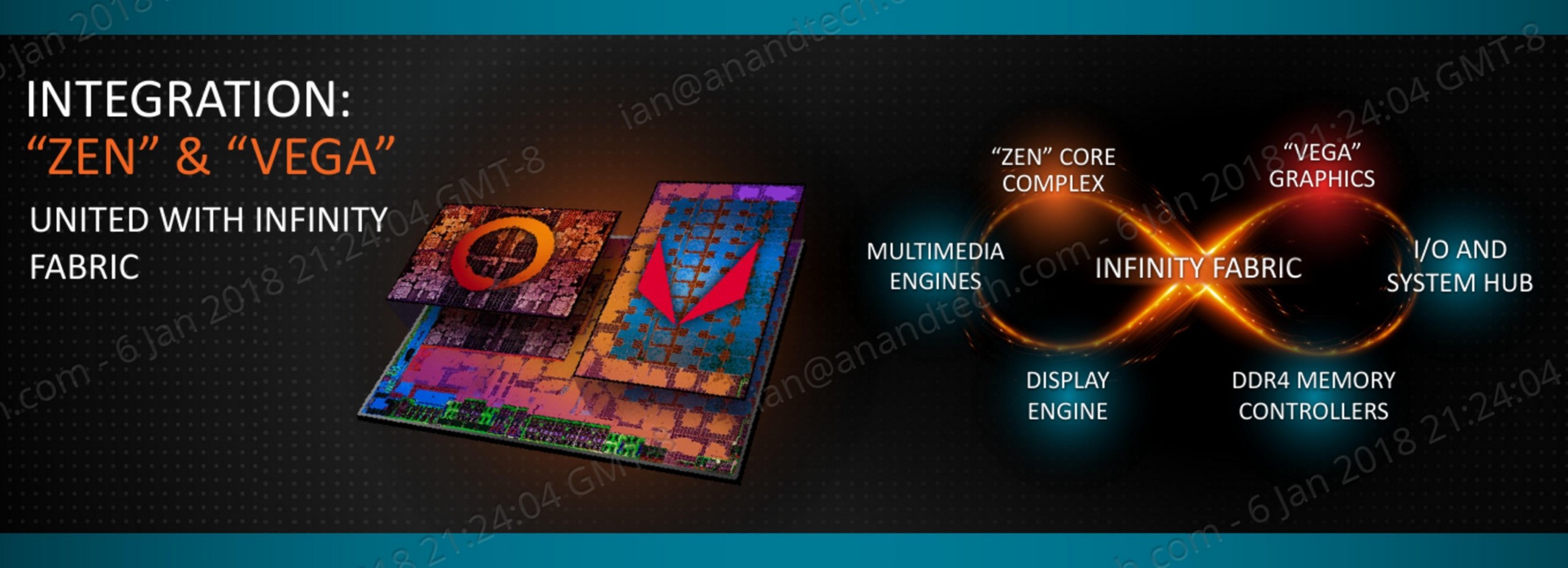
At the heart of both of these designs is the combination of AMD’s first-generation Zen cores, specifically four cores in a ‘core complex’, connected to Vega-based graphics integrated into the silicon. The two units are connected via AMD’s Infinity Fabric, designed for high-bandwidth and scale, and a feature that permeates through AMD’s recent product portfolio.
Ryzen Mobile
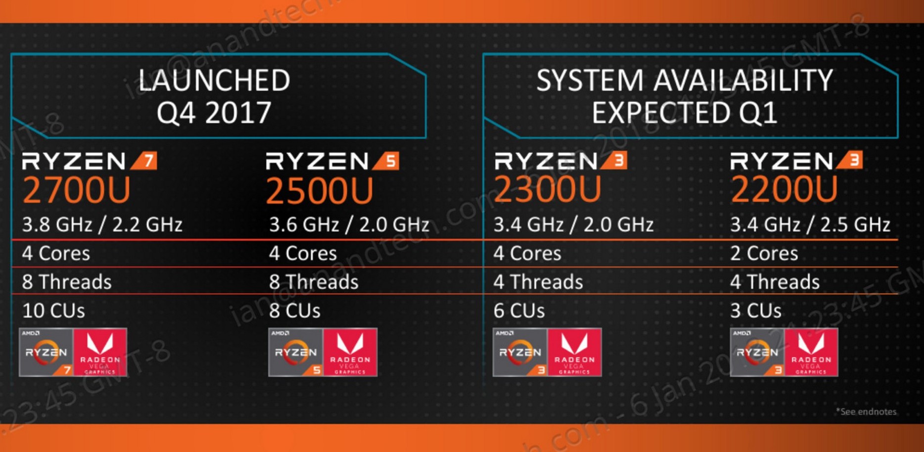
To date, AMD has already announced two products using this configuration. Both of them are for Ryzen Mobile, specifically the Ryzen 7 2700U and Ryzen 5 2500U, which have already been pre-announced in devices such as the HP Envy x2, the Lenovo Ideapad 720S, and the Acer Swift 3. Only the HP Envy x2 has been launched into the market so far (with mixed reviews due to the OEM design, which draws similar criticisms when equipped with Intel CPUs), with the others to see light in Q1 as well as other OEMs like Dell.
The first announcement is regarding adding more Ryzen Mobile processors to the family to cater for a wider audience. To pair with the Ryzen 7 Mobile and Ryzen 5 Mobile, AMD has two Ryzen 3 Mobile parts which will formally be available on January 9th with expected system availability within Q1.
| AMD Ryzen Mobile APUs | |||||
| Ryzen 7 2700U with Vega 10 |
Ryzen 5 2500U with Vega 8 |
Ryzen 3 2300U with Vega 6 |
Ryzen 3 2200U with Vega 3 |
FX-9800P (2015) |
|
| CPU | 4C / 8T 2.2 GHz Base 3.8 GHz Turbo Zen 14nm |
4C / 8T 2.0 GHz Base 3.8 GHz Turbo Zen 14nm |
4C / 4T 2.0 GHz Base 3.4 GHz Turbo Zen 14nm |
2C / 4T 2.5 GHz Base 3.4 GHz Turbo Zen 14nm |
Dual Module 2.7 GHz Base 3.6 GHz Turbo Excavator 28nm |
| GPU | Vega 10 10 CUs 640 SPs < 1300 MHz |
Vega 8 8 CUs 512 SPs < 1100 MHz |
Vega 6 6 CUs 384 SPs |
Vega 3 3 CUs 192 SPs |
GCN 1.2 8 CUs 512 SPs > 758 MHz |
| TDP | 15W | 15W | 15 W | 15 W | 15W |
| DRAM | Up to DDR4-2400 | DDR4-1866 | |||
| L2 Cache | 512 KB/core | 1 MB/module | |||
| L3 Cache | 1 MB/core | 4 MB/core | - | ||
| PCIe Lanes | ? | ? | ? | ? | 8 x PCIe 3.0 |
| Die Size | 209.78 mm2 | 250.4 mm2 | |||
| Transistors | 4.95 billion | 3.1 billion | |||
| Launch | October 2017 | January 2018 | May 2016 | ||
The Ryzen 3 2300U is a quad-core processor without simultaneous multithreading, which separates it from the other components. The base frequency of 2.0 GHz, a top turbo of 3.4 GHz, and a total of six compute units in the Vega graphics (this equates to 384 streaming processors). The Ryzen 3 2300U shares the same TDP as the other parts, coming in at 15W, and AMD wants to position this as a high-performance part for eSports capable notebooks, handily beating anything from Intel’s 7th Generation family.
The Ryzen 3 2200U is the only dual core component in AMD’s entire Ryzen product line, although it does have simultaneous multithreading to give it four threads in total. Having two fewer cores to fire up does give it a boost on the base frequency, coming in at 2.5 GHz, but the turbo frequency matches the other Ryzen 3 at 3.4 GHz. The 2200U is certainly the processor bringing up the rear, with only three compute units (192 streaming processors) in total, and helping AMD shift some of the processors that are not binned as aggressively as the higher-performance units.
AMD is promoting these two processors as capable elements of an entry level 15W notebook that can process DirectX 12, offer advanced video features, and be used in aesthetically pleasing designs with a long battery life, including 2-in-1s, ultrathin notebooks, and gaming laptops.
New Devices
Not to be content with just announcing a couple of new Ryzen Mobile processors, AMD was eager to promote new mobile devices that will be using Ryzen Mobile. To accompany the HP Envy x360, the Lenovo Ideapad 720S, and the Acer Swift 3, Q1 will see the launch of a new HP (under embargo until later this week), the Acer Nitro 5 series, and the Dell Inspiron 5000 series.

Acer’s Nitro line of laptops is typically aimed at the gaming crowd. The Nitro 5 dictates a 15.6-inch display, which in this case is a 1920x1080 IPS panel. Acer will use the pre-announced higher-end APUs, the Ryzen 7 2700U and Ryzen 5 2500U, but will also be pairing this with a Radeon RX 560 graphics chip. We were told by AMD that the integrated graphics and discrete graphics will be used in a switching context: for video playback, the lower power integrated graphics is used and the discrete is disabled, however the discrete graphics is fired up for gaming work. For compute, or for games that support multi-adaptor DirectX 12 technologies, both the integrated graphics and the discrete graphics should be available, however this is up to the game/software to implement.

The Dell Inspiron lines are more home/small-medium business-oriented devices, and here Dell is also using the Ryzen 7 2700U and Ryzen 5 2500U processors to offer peak Mobile APU performance. Designed more as a workhorse than for aesthetics, the Inspiron 5000 will offer AMD parts with 15.6-inch and 17-inch displays in a chassis that can support dual HDD/SSD options. The unit also comes with an optional Radeon 530 discrete GPU, which has 384 compute units based on AMD’s older GCN 1.0 architecture. This comes across as very odd, given that even the Ryzen 5 has 512 compute units of the newer Vega architecture. I can only assume that this provides extra displays for very specific customers, though for most it would seem an overly pointless addition.


131 Comments
View All Comments
A5 - Monday, January 8, 2018 - link
Anything that is forbes.com/sites/* is not credible. You can literally go sign up for one right now if you want.And Forbes proper isn't credible on anything outside the financial industry.
iwod - Monday, January 8, 2018 - link
I mean Christ, you have financial industry reporter reporting on tech they barely understand and having reader that credit a non technical Journal pieces as creditable source and then attacking a journalist on a technical information site labelling him or her and the site as not creditable and when the journalist has a bloody Oxford PhD in the ElecChem Field.LurkingSince97 - Thursday, January 18, 2018 - link
LOL.GloFo announced LONG AGO that they were skipping the 10nm node and going straight from 14nm to 7nm. They mentioned that there would be some 14nm tweaks.
Other competitors started tweaking their 14nm / 16nm nodes and in some cases re-branded them (tsmc, IIRC rebranded a 16nm improvement as 12nm).
There is more than one feature size measurement in a process, being able to shrink a small subset of these by a little bit will allow for some increased density. Add on some other tweaks and you can lower power too. What do you call a heavily tweaked node that only shrinks a few of the feature sizes but not all? What number is half way between 14 and 10?
It doesn't really matter what they call it. Its ~ 10% faster or 10% lower power, with ~10% to 15% higher density.
The 12nm process is essentially a 14nm+, or ++. Its not a wholly new node. Fact 1: it will be incrementally deployed as a revision to the 14nm process where you start over nearly from scratch and almost the entire manufacturing pipeline is new. Fact 2: Unlike most minor tweaks, it does increase density. There is some justification in giving it a new size due to fact 2, but it is not a brand new process due to fact 1.
A truly new node takes _years_ to develop, not months. This appeared on their roadmap suddenly. Everyone and their brother (other than you) knew that they had a 14nm+ in the works -- AMD's roadmaps had "Zen+" on a GloFo "14nm+" node. Suddenly there was no more "14nm+" on AMD's roadmaps, and it was replaced with "12nm".
Significant tweaks to an existing node however,
LurkingSince97 - Thursday, January 18, 2018 - link
Ugh, I should proof-read:Fact 1: it will be incrementally deployed as a revision to the 14nm process where you start over nearly from scratch and almost the entire manufacturing pipeline is new.
Should say:
Fact 1: it will be incrementally deployed as an upgrade to the 14nm process (many of the manufacturing steps remain identical), while an entirely new node typically implies replacing almost the entire manufacturing pipeline.
Sane Indian - Monday, January 8, 2018 - link
"Acer will use the pre-announced higher-end APUs, the Ryzen 7 2700U and Ryzen 5 2500U, but will also be pairing this with a Radeon RX 560 graphics chip."Does iGPU and dGPU can crossfire or they just independently (switch from iGPU to dGPU and vice versa) depending upon power situation.
Ian Cutress - Monday, January 8, 2018 - link
Literally the rest of the paragraph answers the question.We were told by AMD that the integrated graphics and discrete graphics will be used in a switching context: for video playback, the lower power integrated graphics is used and the discrete is disabled, however the discrete graphics is fired up for gaming work. For compute, or for games that support multi-adaptor DirectX 12 technologies, both the integrated graphics and the discrete graphics should be available, however this is up to the game/software to implement.
Kevin G - Monday, January 8, 2018 - link
AMD executing right now and while there is argument that they've played it safe with Zen so far, they are in a very favorable position in the market. -"While most of the roadmap could have been predicted by those of us embedded in this industry, it was good to see AMD volunteering a lot of information. This can be a bit of a double-edged sword, if a competitor knows what you have planned". AMD knows that Intel's roadmap is in chaos as right now and pushing existing Zen designs to lower power envelopes and/or increasing clock speeds will close the performance gap. If Zen 2 advances in terms of IPC by any significant margin, they could actually pull ahead in 2019 but that entirely depends on Intel's response, in particular Ice Lake.Intel's missteps with 10 nm has left them open as the first Cannon Lake parts were due in late 2016! Meltdown and Spectre meltdown could have been the death blow to Cannon Lake as the incoming lawsuits make it unwise to release products with such significant flaws. Intel's server line up is also in chaos due to Meltdown/Spectre as Cascade Lake was pinned in as a stop-gap 14 nm solution before Cannon Lake-SP in 2019. Cascade lake for release this year should already be sampling but Meltdown/Spectre could force a delay. In particular is that Cascade Lake is supposed to support Optane DIMMs. The 10 nm Knight's Hill HPC processor has been cancelled roughly a month ago and replaced by Knight's Mill as a stop-gap for partners looking into AI. We'll probably find out later today when Intel's CEO takes the stage at CES.
wumpus - Monday, January 8, 2018 - link
"Death blow"? You seem to vastly overestimate the amount of silicon GoFlo can produce. Even if everything goes right for AMD, Intel will be shipping Cannon Lake chips left and right to consumers (the chips in the article appeared mostly for consumers) as GoFlo furiously produces Zepplin (or whatever its followup is called) and AMD ships them as hyperprofitable EPYC chips.That said, Intel certainly takes AMD competition seriously enough to throw together competing products such as the X299, even if such products make the rest of Intel look like they have no idea what they are doing. But still, massive gains for AMD will look like a tiny blip in Intel's revenue.
Orenj - Monday, January 8, 2018 - link
With Zen 2 already complete, I'm wondering if it contains any hardware assists for mitigation of Spectre-type attacks a la Intel's proposed IBRS/STIBP/IBPB?PixyMisa - Monday, January 8, 2018 - link
Unlikely; they've only known about this for a couple of months.